The Comprehensive Guide to Ultrasonic PCB Cleaners: Principles, Benefits, and Applications
1. Introduction to Ultrasonic PCB Cleaners
Printed Circuit Boards (PCBs) are essential components in modern electronics, found in everything from consumer gadgets to industrial machinery. Ensuring their cleanliness is crucial for performance, reliability, and longevity. Traditional cleaning methods, such as manual brushing or chemical baths, often fall short in removing microscopic contaminants.
Ultrasonic PCB cleaners offer a superior solution by leveraging high-frequency sound waves to achieve thorough and efficient cleaning. This article explores the working principles, advantages, applications, and best practices for using ultrasonic PCB cleaners.
2. How Ultrasonic PCB Cleaners Work
Ultrasonic cleaning relies on cavitation, a process where high-frequency sound waves generate millions of microscopic bubbles in a liquid cleaning solution. These bubbles implode violently upon contact with the PCB surface, dislodging contaminants such as:
- Flux residues
- Dust and debris
- Oils and greases
- Solder particles
- Oxidation layers
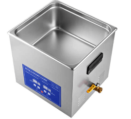
Key Components of an Ultrasonic PCB Cleaner
- Transducer – Converts electrical energy into ultrasonic waves (typically 20–400 kHz).
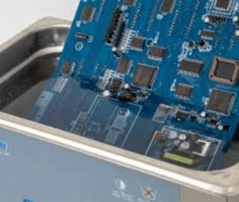
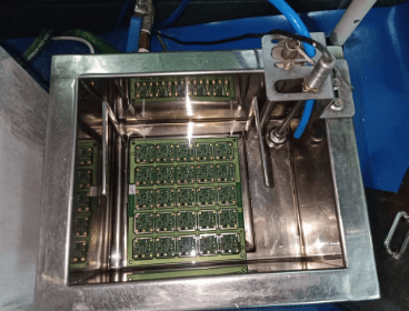
- Cleaning Tank – Holds the PCB and cleaning solution (often isopropyl alcohol, deionized water, or specialized solvents).
- Heater (Optional) – Enhances cleaning efficiency by warming the solution.
- Timer & Controls – Allows users to adjust cleaning duration and intensity.
3. Advantages of Ultrasonic PCB Cleaning
Compared to traditional methods, ultrasonic cleaning offers several benefits:
3.1. Superior Cleaning Performance
- Removes sub-micron particles that brushes or sprays cannot reach.
- Effective in cleaning complex geometries, including tiny vias and under components.
3.2. Non-Destructive Cleaning
- Gentle on delicate components, unlike abrasive scrubbing.
- Does not damage solder joints or thin traces when used correctly.
3.3. Time and Cost Efficiency
- Reduces manual labor and speeds up production.
- Extends PCB lifespan by preventing corrosion and electrical failures.
3.4. Environmentally Friendly Options
- Many modern ultrasonic cleaners use biodegradable, low-toxicity solutions.
- Reduces chemical waste compared to traditional solvent baths.
4. Applications of Ultrasonic PCB Cleaners
Ultrasonic cleaning is widely used across industries:
4.1. Electronics Manufacturing
- Post-solder flux removal – Ensures reliable connections.
- Pre-assembly cleaning – Eliminates contaminants before component placement.
4.2. Automotive & Aerospace Electronics
- Cleans PCBs exposed to harsh environments (dust, moisture, vibrations).
4.3. Medical & Military Electronics
- Ensures high reliability in critical applications.
4.4. Repair & Maintenance
- Restores old or contaminated PCBs for reuse.
5. Best Practices for Ultrasonic PCB Cleaning
To maximize effectiveness and avoid damage, follow these guidelines:
5.1. Selecting the Right Cleaning Solution
- For flux removal – Use alcohol-based or flux-specific cleaners.
- For general cleaning – Deionized water with mild detergents.
- Avoid highly corrosive chemicals that may harm components.
5.2. Optimal Frequency & Power Settings
- Low frequency (20–40 kHz) – Best for heavy contaminants.
- High frequency (80–400 kHz) – Ideal for delicate PCBs with fine features.
5.3. Proper PCB Handling
- Secure PCBs in a basket to prevent collisions with the tank walls.
- Avoid prolonged exposure (typically 3–10 minutes is sufficient).
5.4. Post-Cleaning Steps
- Rinse with distilled water to remove residual chemicals.
- Dry using compressed air or an oven (low temperature).
6. Potential Risks & How to Mitigate Them
While ultrasonic cleaning is highly effective, improper use can cause issues:
6.1. Component Damage
- Ceramic capacitors & MEMS devices may crack under excessive cavitation.
- Solution: Use lower frequencies (<40 kHz) or shorter cleaning cycles.
6.2. Water Intrusion
- Unsealed connectors or batteries can absorb liquid.
- Solution: Mask sensitive areas or use conformal coating.
6.3. Chemical Residues
- Some solvents leave behind harmful residues.
- Solution: Always rinse and dry PCBs thoroughly.
7. Comparing Ultrasonic Cleaning with Alternative Methods
| Method | Effectiveness | Speed | Risk of Damage | Cost |
|---|---|---|---|---|
| Ultrasonic Cleaning | Excellent (microscopic cleaning) | Fast | Low (if used correctly) | Moderate |
| Manual Brushing | Poor (misses small particles) | Slow | High (abrasion risk) | Low |
| Spray Cleaning | Moderate (uneven coverage) | Medium | Medium (chemical exposure) | Low |
| Vapor Degreasing | Good (for oils/grease) | Fast | High (harsh solvents) | High |
8. Future Trends in Ultrasonic PCB Cleaning
- Automated inline systems – Integration with PCB assembly lines.
- Eco-friendly solutions – Water-based and biodegradable cleaners.
- Smart ultrasonic cleaners – AI-powered adjustments for optimal cleaning.
9. Conclusion
Ultrasonic PCB cleaners provide an efficient, reliable, and non-destructive method for removing contaminants from circuit boards. By understanding their working principles, benefits, and best practices, manufacturers and technicians can enhance PCB performance, reduce failure rates, and improve product longevity.
As technology evolves, ultrasonic cleaning will continue to play a vital role in electronics manufacturing, repair, and maintenance—ensuring cleaner, more reliable PCBs for future innovations.