The Design and Manufacturing of IoT Equipment PCBs: Key Considerations and Best Practices
Introduction to IoT PCBs
The Internet of Things (IoT) has revolutionized how devices communicate and operate in our increasingly connected world. At the heart of every IoT device lies its printed circuit board (PCB), which serves as the foundational platform for all electronic components and connectivity features. IoT equipment PCBs differ significantly from traditional circuit boards due to their unique requirements for size, power efficiency, wireless connectivity, and often harsh operating environments.
As IoT applications continue to expand across industries—from smart home devices and wearables to industrial sensors and healthcare monitors—the design and manufacturing of IoT PCBs have become specialized disciplines requiring careful consideration of multiple technical factors. This article explores the critical aspects of IoT PCB development, including design challenges, material selection, manufacturing processes, and testing methodologies that ensure reliability in diverse IoT applications.
Key Design Considerations for IoT PCBs
Size and Form Factor Constraints
One of the most distinctive characteristics of IoT devices is their often compact size, which directly translates to stringent requirements for PCB dimensions. Designers must implement several strategies to accommodate all necessary functionality within limited space:
High-density interconnect (HDI) technology enables more circuitry in smaller areas by utilizing finer lines and spaces, microvias, and buried vias. This approach allows for component placement on both sides of the board and more efficient routing in multilayer designs.
Component selection plays a crucial role in miniaturization. Surface-mount devices (SMDs) with smaller footprints, chip-scale packages, and even bare die implementations help reduce the overall PCB size. The use of multi-function ICs that combine several features (like microcontroller + radio or sensor + processor) can significantly decrease component count.
Board shape flexibility is another consideration, as many IoT devices require non-rectangular PCBs to fit into product enclosures. This may involve designing odd-shaped boards with cutouts or flexible PCBs that can bend to accommodate product form factors.
Power Management and Efficiency
Most IoT devices operate on battery power, making energy efficiency a paramount concern in PCB design:
Low-power circuit design techniques include selecting components with low quiescent current, implementing proper power domains that can be turned off when not in use, and optimizing clock speeds based on processing requirements.
Power supply design must be highly efficient, often incorporating switch-mode power supplies (SMPS) with high conversion efficiency even at low loads. Careful layout of power rails and proper decoupling capacitor placement are essential to minimize losses.
Energy harvesting considerations are becoming increasingly important for certain IoT applications. PCBs may need to incorporate circuits for solar, thermal, or RF energy harvesting, requiring specialized components and layout techniques.
Wireless Connectivity Implementation
Connectivity is what makes an IoT device part of the “Internet of Things,” and the PCB must properly support the chosen communication protocol:
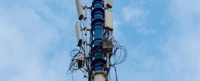
Antenna design and placement is critical for reliable wireless performance. The PCB may incorporate printed antennas, antenna matching circuits, and careful RF trace routing to maintain impedance control. Keep-out areas and proper grounding around antennas are essential.
Multiple radio coexistence is a common requirement for IoT devices that need to support Bluetooth, Wi-Fi, cellular, or other protocols simultaneously. This requires careful frequency planning, shielding, and filtering to prevent interference.
Signal integrity must be maintained throughout all high-frequency circuits. This involves controlled impedance routing, proper layer stacking, and minimization of vias in RF paths. Electromagnetic compatibility (EMC) considerations are vital for both emissions and immunity.
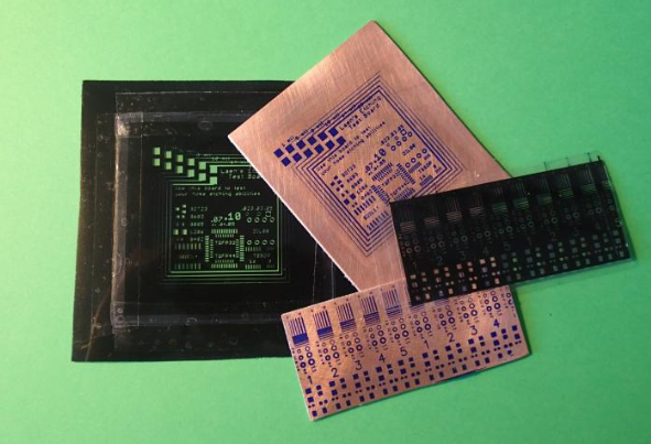
Material Selection for IoT PCBs
Substrate Materials
The choice of PCB substrate material significantly impacts the performance, reliability, and cost of IoT devices:
FR-4, the most common PCB material, is suitable for many IoT applications due to its good balance of performance and cost. However, standard FR-4 may not be adequate for high-frequency or high-reliability applications.
High-frequency laminates like Rogers or Taconic materials are often necessary for RF circuits operating at 2.4 GHz or higher. These materials provide stable dielectric constants and low loss tangents for better signal integrity.
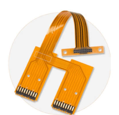
Flexible substrates such as polyimide are used in wearable IoT devices or applications where the PCB needs to bend. These materials allow for three-dimensional packaging solutions but require different design and manufacturing approaches.
Ceramic substrates may be used in high-temperature or high-power IoT applications, though they are less common due to higher costs.
Surface Finishes
The PCB surface finish affects solderability, durability, and performance:
ENIG (Electroless Nickel Immersion Gold) provides a flat surface excellent for fine-pitch components and has good shelf life, though it’s more expensive than some alternatives.
Immersion Silver offers good solderability at lower cost than ENIG and performs well for high-frequency applications, but can tarnish over time.
OSP (Organic Solderability Preservative) is cost-effective and works well for simple designs but has limited shelf life and isn’t suitable for multiple reflow cycles.
ENEPIG (Electroless Nickel Electroless Palladium Immersion Gold) provides the best wire-bonding capability and excellent reliability for harsh environments, though at premium cost.
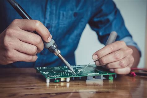
Manufacturing and Assembly Challenges
Miniaturization Challenges
The small size of IoT PCBs presents several manufacturing difficulties:
Fine-pitch component placement requires high-precision pick-and-place machines and careful solder paste application. 01005 and even smaller component sizes are becoming common in IoT designs.
Microvia drilling and plating for HDI boards demands specialized equipment and processes to ensure reliability, especially for stacked or staggered via configurations.
Solder joint inspection becomes more challenging with smaller components, often necessitating automated optical inspection (AOI) or even X-ray inspection for hidden joints.
Mixed Technology Assembly
Many IoT PCBs incorporate a mix of technologies that complicate assembly:
Through-hole components may still be needed for connectors or certain power components alongside predominantly surface-mount designs.
Bottom-side components are frequently used to maximize space utilization, requiring careful handling during reflow to prevent parts from falling off.
Embedded components, where passive elements are buried within the PCB layers, are becoming more common in high-end IoT devices to save space and improve performance.
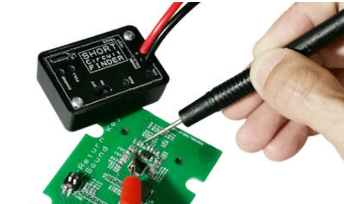
Testing and Quality Assurance
Ensuring quality in IoT PCB manufacturing requires specialized approaches:
Flying probe testing is often used instead of bed-of-nails fixtures for small production runs or highly compact designs where test point access is limited.
RF testing verifies the performance of wireless circuits, including antenna radiation patterns, transmitter power, and receiver sensitivity.
Power consumption testing validates that the PCB meets its energy efficiency targets across all operational modes.
Environmental stress testing subjects boards to temperature cycling, humidity exposure, and vibration to ensure reliability in field conditions
Reliability Considerations for IoT Applications
Harsh Environment Operation
Many IoT devices operate in challenging conditions that affect PCB reliability:
Temperature extremes require careful selection of components and materials with appropriate operating ranges. Thermal management through proper layout and, in some cases, thermal vias may be necessary.
Humidity and moisture resistance can be addressed through conformal coatings, hydrophobic nano-coatings, or selection of moisture-resistant materials.
Mechanical stress in industrial or automotive applications may necessitate thicker boards, strategic stiffening, or flexible PCB solutions.
Long-term Reliability
IoT devices often need to operate maintenance-free for years:
Electrochemical migration prevention involves proper cleaning to remove flux residues and adequate spacing between high-voltage differences.
Tin whisker mitigation may require avoiding pure tin finishes in favor of tin alloys or other surface treatments.
Component aging considerations are important, particularly for electrolytic capacitors and other parts with limited lifetimes.
Future Trends in IoT PCB Technology
Advanced Integration Techniques
System-in-Package (SiP) technologies are allowing more functionality to be integrated into smaller spaces by combining multiple dies in a single package.
Embedded active components represent the next step beyond embedded passives, with ICs being placed within the PCB layers themselves.
3D printed electronics are emerging as a potential solution for highly customized IoT device geometries and rapid prototyping.
Sustainable Materials and Processes
Biodegradable substrates are being developed for environmentally conscious IoT applications where device recycling is challenging.
Lead-free and halogen-free materials continue to evolve to meet environmental regulations without compromising performance.
Low-energy manufacturing processes are gaining attention as the IoT industry addresses its overall environmental impact.
Conclusion
The design and manufacturing of PCBs for IoT equipment present unique challenges that require specialized knowledge and careful attention to detail. From size constraints and power efficiency to wireless performance and reliability in harsh environments, IoT PCBs demand a holistic approach that balances competing requirements.
As IoT applications continue to proliferate across industries, PCB technologies are evolving to meet these demands through advanced materials, innovative design techniques, and precision manufacturing processes. Successful IoT PCB development requires close collaboration between designers, component suppliers, and manufacturing partners to create solutions that are not only functional but also reliable, cost-effective, and suitable for mass production.
By understanding and addressing the key considerations outlined in this article, electronics engineers can develop IoT PCBs that power the next generation of connected devices, enabling the continued expansion of the Internet of Things into every aspect of modern life.