The Design of a Charger Circuit PCB: An In-Depth Exploration
Introduction
Printed Circuit Board (PCB) design for charger circuits represents a fascinating intersection of electrical engineering, thermal management, and industrial design. In our increasingly mobile world, efficient and reliable charger circuits have become essential components of daily life, powering everything from smartphones to electric vehicles. This article examines the intricate process of designing a charger circuit PCB, exploring the schematic considerations, component selection, layout strategies, and manufacturing concerns that transform theoretical electrical designs into practical, high-performance charging solutions.
Fundamental Components of Charger Circuit PCBs
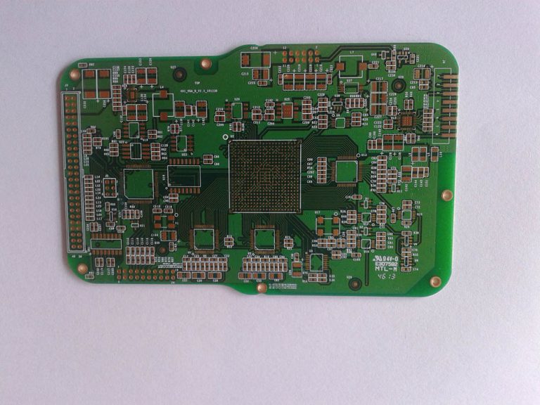
At its core, a charger circuit PCB integrates several critical components that work in harmony to convert and regulate electrical power:
Power Input Stage: This section typically includes connectors, fuses, and transient voltage suppression components that interface with the external power source. For AC-DC chargers, this stage begins with rectification components that convert alternating current to direct current. The input stage must be designed with appropriate safety margins to handle voltage spikes and electrical noise present in typical power lines.
Conversion and Regulation Circuitry: The heart of the charger, this section contains the switching components (MOSFETs or transistors), control ICs, and supporting passive components that regulate voltage and current to the required charging specifications. Modern charger designs often employ switch-mode power supply (SMPS) topologies like flyback, buck, or boost converters for their efficiency advantages over linear regulators.
Output Stage: This portion delivers the processed power to the device being charged, featuring output connectors, filtering capacitors, and often current-limiting or smart charging ICs that communicate with the connected device. USB Power Delivery (USB-PD) compliant chargers include sophisticated communication chips that negotiate voltage and current levels with the powered device.
Control and Feedback Networks: Critical for maintaining stable operation, these circuits include voltage dividers, current sense resistors, optocouplers (in isolated designs), and feedback loops that allow the control IC to adjust operation based on output conditions. Precision in these components directly affects charging accuracy and safety.
Ancillary Circuits: Many modern chargers incorporate additional functionality such as status indicators (LEDs or displays), thermal monitoring circuits, and in advanced designs, wireless communication modules for smart charging features.
Schematic Design Considerations
Developing the schematic for a charger circuit PCB requires careful attention to several key factors:
Topology Selection: Engineers must choose between various power conversion topologies based on input/output voltage relationships, power requirements, and efficiency targets. Common choices include buck converters (for stepping down voltage), boost converters (for increasing voltage), and buck-boost configurations for applications requiring both capabilities.
Component Specifications: Each component must be selected to handle expected voltage, current, and power dissipation with appropriate safety margins. Semiconductor devices like diodes and transistors require particular attention to their voltage and current ratings, while passive components must be chosen for their tolerance, temperature coefficient, and frequency characteristics.
Safety and Compliance: Charger circuits must incorporate protections against overvoltage, overcurrent, short circuits, and thermal overload. These protections must meet relevant safety standards such as UL, CE, or IEC specifications depending on the target market. Isolation requirements between primary and secondary circuits in AC-DC chargers demand careful spacing and component selection.
Efficiency Optimization: With growing emphasis on energy efficiency and thermal performance, schematic design must minimize losses through careful selection of low-RDS(on) MOSFETs, high-efficiency rectifiers (like Schottky diodes), and optimal control ICs that support advanced switching techniques.
EMI Mitigation: The schematic should include necessary filtering components to suppress both conducted and radiated electromagnetic interference, crucial for passing regulatory tests and preventing interference with other electronic devices.
PCB Layout Strategies
Translating the schematic into an effective physical layout represents one of the most challenging aspects of charger PCB design:
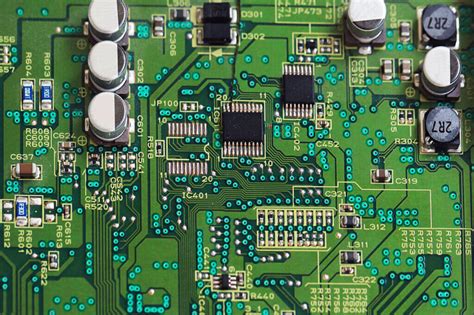
Power Plane Management: The PCB stackup must provide adequate copper thickness and plane allocation for high-current paths. Multi-layer boards often dedicate entire layers to ground and power distribution to minimize impedance and improve thermal performance. Current densities must be calculated to ensure traces and planes can handle expected loads without excessive heating.
Component Placement: Strategic placement begins with positioning the power conversion IC or transformer at the center, surrounded by supporting components in functional blocks. Input filtering components should be located near the power entry points, while output components cluster near the charging port. High-frequency switching components require particular attention to minimize loop areas and reduce EMI.
Thermal Considerations: Power components that generate significant heat must be placed with adequate spacing and thermal relief. The layout should facilitate heat dissipation through thermal vias, copper pours, and in some cases, provisions for heatsinks or thermal interface materials. Temperature-sensitive components should be positioned away from major heat sources.
High-Frequency Considerations: The switching nature of modern charger circuits creates high di/dt and dv/dt conditions that can lead to ringing, overshoot, and EMI. Careful attention must be paid to keeping high-frequency switching loops small, using proper grounding techniques, and implementing appropriate snubber circuits when needed.
Isolation and Creepage: For AC-DC chargers, the layout must maintain proper isolation distances (both creepage and clearance) between primary and secondary sides as specified by safety standards. This often involves creating physical barriers or isolation slots in the PCB and using reinforced insulation techniques.
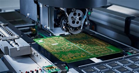
Manufacturing Constraints: The layout must account for production realities including solder mask requirements, component package sizes, assembly processes (wave soldering vs. reflow), and test point accessibility. Design for Manufacturing (DFM) and Design for Test (DFT) principles help ensure reliable, cost-effective production.
Advanced Design Techniques
Contemporary charger PCB designs incorporate several advanced techniques to meet increasing performance demands:
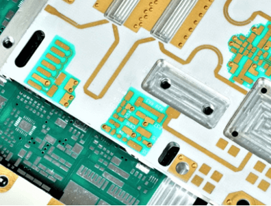
Multilayer PCB Architectures: High-density charger designs often employ 4-8 layer boards, allowing for dedicated power and ground planes, controlled impedance traces, and better EMI performance. Layer stacking must be optimized for both electrical and thermal performance.
Embedded Components: Some advanced designs embed passive components within the PCB layers to save space and reduce parasitic inductance. This technique is particularly valuable in compact charger designs where board real estate is limited.
3D Component Placement: With the growing popularity of gallium nitride (GaN) and silicon carbide (SiC) power devices that operate at higher frequencies, designers must consider the three-dimensional aspects of component placement and interconnections to minimize parasitic effects.
Thermal Via Arrays: Dense arrays of thermal vias under power components help transfer heat to inner layers or opposite sides of the board where it can be more effectively dissipated. These via patterns must be carefully designed to balance thermal transfer with structural integrity.
Advanced Materials: For high-power or high-frequency applications, designers may select specialized PCB materials with better thermal conductivity or dielectric properties than standard FR-4, such as metal-core boards or high-frequency laminates.
Testing and Validation
Before mass production, charger circuit PCBs undergo rigorous testing:
Electrical Testing: Verification of input/output characteristics, efficiency measurements, load regulation, and line regulation under various operating conditions. This includes testing protection circuits by simulating fault conditions.
Thermal Testing: Evaluation of temperature rise under maximum load conditions using thermal imaging or strategically placed thermocouples. Components must remain within specified temperature limits during continuous operation.
EMI/EMC Testing: Compliance testing for conducted and radiated emissions, as well as immunity to external interference. Pre-compliance testing during design helps identify and mitigate potential issues early.
Safety Certification: Formal testing by certified laboratories to verify compliance with relevant safety standards, including dielectric strength tests, fault condition tests, and construction evaluations.
Reliability Testing: Extended operation under various environmental conditions (temperature, humidity) to verify long-term reliability and identify potential failure modes.
Future Trends in Charger PCB Design
The field of charger PCB design continues to evolve with several emerging trends:
GaN and SiC Technology: Wide-bandgap semiconductors enable smaller, more efficient chargers operating at higher frequencies, requiring new approaches to PCB layout and thermal management.
Higher Power Density: Consumer demand for faster charging in smaller form factors drives innovation in component integration and thermal solutions.
USB Power Delivery: The widespread adoption of USB-PD standards requires more sophisticated control circuitry and flexible output capabilities within charger designs.
Wireless Charging Integration: Some designs now incorporate both wired and wireless charging capabilities on a single PCB, presenting new layout challenges.
Sustainable Design: Increasing focus on recyclability and use of environmentally friendly materials in PCB construction.
Conclusion
The design of a charger circuit PCB represents a complex engineering challenge that balances electrical performance, thermal management, safety compliance, and manufacturability. From the initial schematic capture through final layout and testing, each decision impacts the charger’s efficiency, reliability, and cost. As charging technology continues to advance, PCB designers must adapt to new components, higher performance requirements, and evolving standards. The meticulous attention to detail required in charger PCB design ensures that these ubiquitous devices safely and efficiently power our modern mobile lives, often in increasingly compact and sophisticated form factors. Understanding the principles and practices behind charger PCB design provides valuable insight into one of the most crucial yet often overlooked aspects of contemporary electronics.