The Difference Between PCB and PCBA: A Comprehensive Analysis
Introduction
In the world of electronics manufacturing, the terms PCB (Printed Circuit Board) and PCBA (Printed Circuit Board Assembly) are often used interchangeably, but they refer to distinct stages in the production process. Understanding the difference between PCB and PCBA is crucial for anyone involved in electronics design, manufacturing, or procurement. This article will delve into the definitions, processes, and key differences between PCB and PCBA, providing a comprehensive understanding of each.
1. Definition of PCB
1.1. What is a PCB?
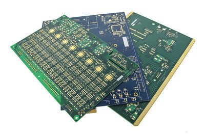
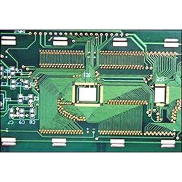
A Printed Circuit Board (PCB) is the foundational component of most electronic devices. It is a flat board made of insulating material, such as fiberglass, with conductive pathways etched or printed onto its surface. These pathways, known as traces, connect various electronic components, such as resistors, capacitors, and integrated circuits (ICs), to form a functional circuit.
1.2. Types of PCBs
PCBs come in various types, each suited for different applications:
- Single-Layer PCBs: These have conductive traces on only one side of the board. They are simple and cost-effective, suitable for basic electronic devices.
- Double-Layer PCBs: These have conductive traces on both sides of the board, allowing for more complex circuits.
- Multi-Layer PCBs: These consist of multiple layers of conductive traces separated by insulating material. They are used in highly complex and compact devices, such as smartphones and computers.
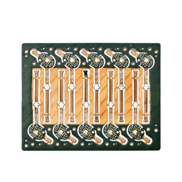
- Flexible PCBs: These are made of flexible materials, allowing them to bend and fit into unconventional shapes. They are used in applications where space and flexibility are critical.
- Rigid-Flex PCBs: These combine rigid and flexible layers, offering both stability and flexibility. They are used in advanced applications, such as aerospace and medical devices.
2. Definition of PCBA
2.1. What is a PCBA?
A Printed Circuit Board Assembly (PCBA) refers to a PCB that has been populated with electronic components and is ready for use in an electronic device. The process of assembling components onto a PCB involves several steps, including soldering, inspection, and testing. The result is a fully functional circuit board that can be integrated into a larger electronic system.
2.2. Types of PCBA
The assembly process can vary depending on the complexity of the PCB and the components involved:
- Through-Hole Technology (THT): In this method, component leads are inserted into drilled holes on the PCB and soldered onto pads on the opposite side. THT is reliable and suitable for larger components.
- Surface Mount Technology (SMT): In this method, components are placed directly onto the surface of the PCB and soldered using reflow soldering. SMT allows for smaller components and higher density, making it ideal for modern, compact devices.
- Mixed Technology: Some PCBAs use a combination of THT and SMT, leveraging the strengths of both methods.
3. Key Differences Between PCB and PCBA
3.1. Stage in the Manufacturing Process
The most fundamental difference between PCB and PCBA is their stage in the manufacturing process. A PCB is the bare board with conductive traces but no components. It is the substrate upon which electronic components are mounted. In contrast, a PCBA is the completed assembly, with all components soldered onto the PCB, ready for integration into an electronic device.
3.2. Complexity and Functionality
A PCB is a passive component; it does not perform any function on its own. Its role is to provide the electrical connections between components. A PCBA, on the other hand, is an active component. It is a fully functional circuit that can perform specific tasks, such as processing signals, storing data, or controlling other components.
3.3. Manufacturing Processes
The manufacturing processes for PCB and PCBA are distinct:
- PCB Manufacturing: This involves designing the circuit layout, printing the conductive traces, and etching the board. The process requires precision and attention to detail to ensure the integrity of the electrical connections.
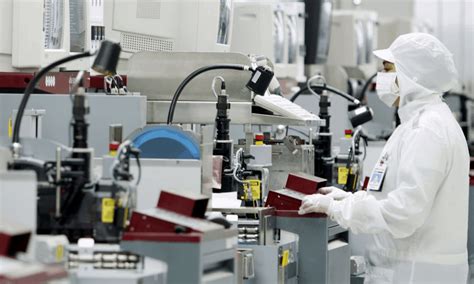
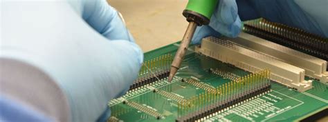
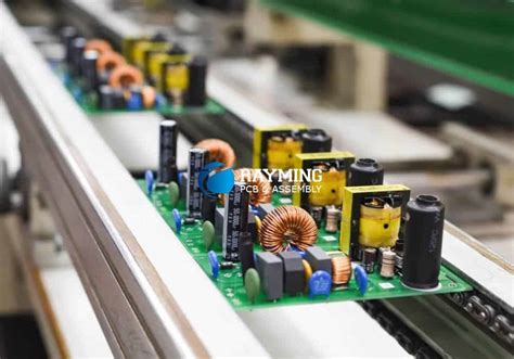
- PCBA Manufacturing: This involves placing and soldering components onto the PCB. The process includes several steps, such as solder paste application, component placement, reflow soldering, inspection, and testing. Each step must be carefully controlled to ensure the quality and reliability of the final assembly.
4. Design Considerations for PCB and PCBA
4.1. PCB Design Considerations
Designing a PCB involves several critical considerations:
- Layer Stackup: The number and arrangement of layers in a multi-layer PCB must be carefully planned to optimize signal integrity and thermal management.
- Trace Routing: The layout of conductive traces must minimize signal interference and ensure efficient power distribution.
- Component Placement: The placement of components on the PCB must consider factors such as thermal management, signal integrity, and manufacturability.
- Design for Manufacturability (DFM): The PCB design must be compatible with the manufacturing processes, ensuring that it can be produced reliably and cost-effectively.
4.2. PCBA Design Considerations
Designing a PCBA involves additional considerations beyond those for a PCB:
- Component Selection: The choice of components must consider factors such as performance, reliability, and availability. Components must also be compatible with the chosen assembly method (THT, SMT, or mixed).
- Soldering Process: The soldering process must be carefully controlled to ensure strong, reliable connections. This includes selecting the appropriate solder paste, reflow profile, and inspection methods.
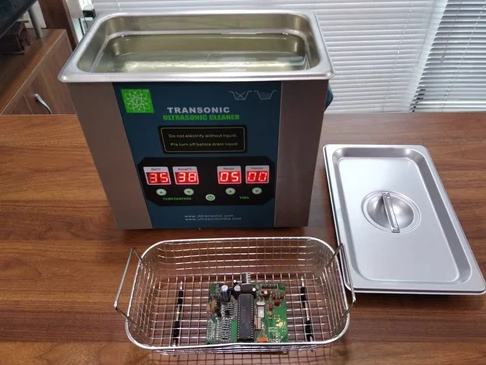
- Testing and Inspection: The PCBA must undergo rigorous testing and inspection to ensure functionality and reliability. This includes electrical testing, functional testing, and visual inspection.
5. Quality Control and Testing
5.1. PCB Quality Control
Quality control for PCBs involves several steps:
- Visual Inspection: The PCB is inspected for defects such as shorts, opens, and misaligned traces.
- Electrical Testing: The PCB undergoes electrical testing to verify the integrity of the conductive traces and ensure there are no shorts or opens.
- Dimensional Inspection: The PCB is measured to ensure it meets the specified dimensions and tolerances.
5.2. PCBA Quality Control
Quality control for PCBAs is more complex and involves additional steps:
- Solder Paste Inspection (SPI): The solder paste application is inspected to ensure proper volume, alignment, and coverage.
- Automated Optical Inspection (AOI): The assembled PCB is inspected using automated optical systems to detect defects such as missing components, misaligned components, and solder bridges.
- X-Ray Inspection: X-ray inspection is used to detect defects in hidden solder joints, such as those in Ball Grid Array (BGA) components.
- Functional Testing: The PCBA undergoes functional testing to verify that it performs as intended. This may include power-on testing, signal testing, and environmental testing.
6. Applications of PCB and PCBA
6.1. PCB Applications
PCBs are used in a wide range of applications, from simple consumer electronics to complex industrial systems. Some common applications include:
- Consumer Electronics: Smartphones, tablets, laptops, and televisions.
- Industrial Equipment: Control systems, power supplies, and automation equipment.
- Medical Devices: Diagnostic equipment, imaging systems, and patient monitoring devices.
- Automotive Systems: Engine control units, infotainment systems, and advanced driver-assistance systems (ADAS).
6.2. PCBA Applications
PCBAs are used in the same applications as PCBs but represent the functional, assembled version of the board. Some specific examples include:
- Consumer Electronics: Assembled motherboards, power supplies, and display drivers in smartphones and laptops.
- Industrial Equipment: Fully assembled control panels, motor drives, and sensors.
- Medical Devices: Complete diagnostic machines, imaging systems, and wearable health monitors.
- Automotive Systems: Fully integrated engine control units, infotainment systems, and ADAS modules.
7. Conclusion
In summary, while PCB and PCBA are closely related, they represent distinct stages in the electronics manufacturing process. A PCB is the bare board with conductive traces, serving as the foundation for electronic circuits. A PCBA is the completed assembly, with all components soldered onto the PCB, ready for use in an electronic device. Understanding the differences between PCB and PCBA is essential for anyone involved in electronics design, manufacturing, or procurement. By considering the unique requirements and challenges of each stage, manufacturers can ensure the production of high-quality, reliable electronic devices that meet the demands of today’s technology-driven world.