The Difference Between PCB Positive and Negative Film: A Comprehensive Guide
Introduction to PCB Film Types
In printed circuit board (PCB) manufacturing, the terms “positive film” and “negative film” refer to two distinct photographic methods used to transfer circuit patterns onto copper-clad boards. These techniques play a fundamental role in determining how copper is either retained or removed during the etching process. Understanding the difference between positive and negative film is crucial for PCB designers and manufacturers, as the choice between them affects the board’s fabrication process, cost, and final quality.
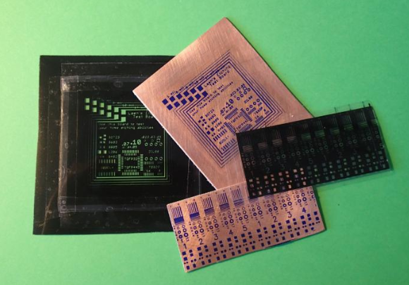
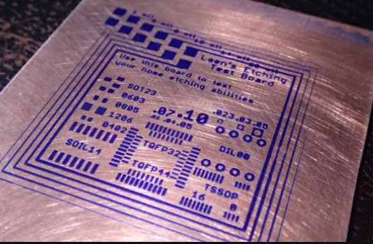
Photographic films in PCB production serve as stencils that either block or allow light to pass through during the exposure process. This light exposure chemically alters the photoresist coating on the copper board, creating a pattern that will guide the subsequent etching or plating processes. While modern PCB manufacturing increasingly uses direct imaging techniques that eliminate the need for physical films, the concepts of positive and negative imaging remain relevant as they form the basis of these digital methods.
Understanding Positive Film in PCB Manufacturing
Definition and Characteristics
Positive film, in PCB terminology, creates a direct correlation between the opaque areas on the film and the copper that remains on the final board. When using positive film:
- The black (opaque) areas on the film represent the copper traces that will remain after etching
- The clear (transparent) areas correspond to where copper will be removed
- The photoresist under the opaque areas remains soluble after exposure
- The photoresist under clear areas becomes insoluble after exposure
This method is called “positive” because the image on the film matches the positive image of the final copper pattern—what you see on the film is what you get on the board.
The Positive Film Process
The manufacturing sequence with positive film typically follows these steps:
- Application of Positive Photoresist: The copper-clad laminate is coated with a light-sensitive positive photoresist.
- Exposure: The film is placed over the board and exposed to UV light. Where the film is clear, the photoresist hardens; where opaque, it remains soft.
- Development: The board is developed in a chemical solution that removes the unexposed (soft) photoresist, exposing the copper beneath.
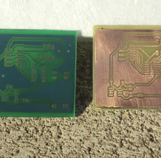
- Etching: The exposed copper is etched away, leaving only the protected copper traces.
- Stripping: The remaining photoresist is removed, revealing the final copper pattern.
Advantages of Positive Film
Positive film offers several benefits in PCB manufacturing:
- Higher Resolution: Generally capable of producing finer lines and spaces
- Better for Complex Designs: More suitable for high-density interconnect (HDI) boards
- Direct Correlation: Easier to visualize as the film matches the final copper pattern
- Wider Process Window: More forgiving in exposure and development parameters
Common Applications
Positive film is typically used for:
- High-precision PCBs with fine features
- Multilayer boards with tight tolerances
- HDI and microvia technology
- Boards requiring impedance control
Exploring Negative Film in PCB Production
Definition and Characteristics
Negative film operates on the inverse principle of positive film:
- The clear (transparent) areas on the film represent the copper that will remain
- The black (opaque) areas correspond to where copper will be removed
- The photoresist under opaque areas remains soluble after exposure
- The photoresist under clear areas becomes insoluble after exposure
This method is called “negative” because the image on the film is the inverse of the final copper pattern—the board ends up with the opposite of what appears on the film.
The Negative Film Process
The manufacturing sequence with negative film follows these steps:
- Application of Negative Photoresist: The copper-clad laminate is coated with negative photoresist.
- Exposure: The film is placed over the board and exposed to UV light. Where the film is clear, the photoresist hardens; where opaque, it remains soft.
- Development: The board is developed in a chemical solution that removes the unexposed (soft) photoresist, exposing the copper beneath.
- Etching: The exposed copper is etched away, leaving only the protected copper traces.
- Stripping: The remaining photoresist is removed, revealing the final copper pattern.
While the steps appear similar to positive film, the key difference lies in the photoresist’s reaction to light and the inverse relationship between the film image and final copper pattern.
Advantages of Negative Film
Negative film offers several distinct advantages:
- Faster Exposure Times: Requires less UV exposure than positive film
- Better Copper Adhesion: The hardened resist tends to adhere more strongly to copper
- More Durable Resist: Better resistance to chemical and mechanical stresses during processing
- Lower Cost: Generally less expensive materials and processes
Common Applications
Negative film is typically used for:
- Single-sided and simple double-sided boards
- High-volume production runs
- Boards with larger features and looser tolerances
- Prototype and quick-turn PCBs
- Thick copper boards
Key Differences Between Positive and Negative Film
Photoresist Chemistry
The fundamental difference lies in the photoresist’s chemical reaction to light:
- Positive Photoresist: Becomes soluble when exposed to light
- Negative Photoresist: Becomes insoluble when exposed to light
This opposite behavior dictates how the resist is developed and what portions of copper are removed during etching.
Image Polarity
The relationship between the film image and final copper pattern is inverted:
- Positive Film: Film image matches copper pattern (1:1 correlation)
- Negative Film: Film image is inverse of copper pattern
Feature Resolution
Positive film generally offers better resolution:
- Positive: Can achieve finer lines (3 mil or less)
- Negative: Typically limited to 5 mil lines or larger
Process Parameters
Several process factors differ between the two methods:
| Parameter | Positive Film | Negative Film |
|---|---|---|
| Exposure Time | Longer | Shorter |
| Development Time | Longer | Shorter |
| Exposure Energy | Higher | Lower |
| Process Control | More critical | More forgiving |
Cost Considerations
Negative film processes are generally more economical:
- Material Costs: Negative photoresist is typically less expensive
- Processing Costs: Faster exposure and development reduce labor and equipment time
- Waste Treatment: Negative processes often generate less chemical waste
Choosing Between Positive and Negative Film
Design Complexity
- Choose Positive Film for:
- High-density designs
- Fine-pitch components
- Controlled impedance requirements
- Complex multilayer boards
- Choose Negative Film for:
- Simple designs
- Larger features
- Single or double-layer boards
- Prototypes and quick turns
Production Volume
- High Volume: Negative film may offer cost advantages
- Low Volume: Positive film provides better flexibility for design changes
Material Considerations
- Thick Copper: Negative film handles thicker copper better
- Flex Circuits: Positive film is generally preferred for flex applications
Equipment Availability
Some manufacturers may be equipped for only one process type, which may dictate the choice.
Modern Alternatives and Future Trends
While photographic films were once the standard in PCB manufacturing, several modern alternatives have emerged:
Direct Imaging (LDI)
Laser Direct Imaging systems project the circuit pattern directly onto the photoresist-coated board without using physical films. However, the concepts of positive and negative resist still apply in these systems.
Dry Film Photoresist
Both positive and negative dry films are available, offering advantages over liquid photoresists in certain applications.
Inkjet Printing
Emerging technologies use inkjet printers to directly apply etch-resistant patterns, potentially eliminating the need for photoresist altogether.
Conclusion
The choice between positive and negative film in PCB manufacturing depends on multiple factors including design complexity, production volume, feature size requirements, and cost considerations. Positive film offers higher resolution and is better suited for complex, high-density designs, while negative film provides economic advantages for simpler boards and high-volume production. Understanding these fundamental differences enables PCB designers and manufacturers to select the most appropriate method for their specific application, ensuring optimal quality, performance, and cost-effectiveness in the final product.
As PCB technology continues to evolve with finer features and more complex designs, positive film processes are becoming increasingly dominant, particularly in advanced applications like HDI and flexible circuits. However, negative film remains a viable and cost-effective solution for many conventional PCB applications. The ongoing development of direct imaging and other digital technologies may eventually make physical films obsolete, but the underlying principles of positive and negative imaging will continue to inform these new manufacturing methodologies.