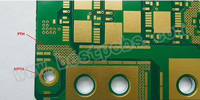
The Difference Between PTH and NPTH in PCB Through-Holes
Introduction
Printed Circuit Boards (PCBs) form the foundation of modern electronics, providing both mechanical support and electrical connections for electronic components. Among the most critical features of any PCB are its through-holes—the drilled holes that allow for component mounting and layer interconnection. These through-holes primarily come in two types: Plated Through-Holes (PTH) and Non-Plated Through-Holes (NPTH). Understanding the differences between PTH and NPTH is essential for PCB designers, manufacturers, and engineers working with circuit boards.
This article provides a comprehensive examination of PTH and NPTH, exploring their structural differences, manufacturing processes, applications, advantages, and limitations. By the end of this discussion, readers will have a clear understanding of when to use each type of through-hole and how their presence affects PCB functionality and reliability.
Definition and Basic Concepts
Plated Through-Holes (PTH)
Plated Through-Holes, commonly abbreviated as PTH, are holes drilled through a PCB that have been electroplated with a conductive material, typically copper. This plating creates an electrical connection between different layers of the board, allowing signals and power to pass from one side of the PCB to the other or between internal layers.
The plating process coats the entire interior surface of the hole, creating a conductive barrel that connects the copper layers the hole passes through. PTHs serve three primary functions:
- Providing electrical connectivity between layers
- Creating mounting points for through-hole components
- Enhancing thermal transfer in some applications
Non-Plated Through-Holes (NPTH)
Non-Plated Through-Holes (NPTH), as the name suggests, are holes drilled through a PCB that do not have any conductive plating on their interior surfaces. These holes remain as simple openings through the board substrate material without establishing electrical connections between layers.
NPTHs are typically used for:
- Mechanical mounting purposes
- Alignment holes for assembly
- Ventilation openings
- Areas requiring electrical isolation
- Special component requirements
Manufacturing Process Differences
PTH Manufacturing Process
The creation of Plated Through-Holes involves a complex, multi-step process that integrates with the overall PCB fabrication:
- Drilling: Holes are drilled through the PCB stack at the required locations using precision CNC drilling machines. For multi-layer boards, this occurs after layer alignment and lamination.
- Deburring and Cleaning: The drilled holes are cleaned to remove any debris or rough edges (burrs) that might interfere with the plating process.
- Electroless Copper Deposition: A thin layer of copper is chemically deposited on all surfaces, including the hole walls. This initial coating provides the conductive base needed for subsequent electroplating.
- Electroplating: The board undergoes electroplating where additional copper is deposited onto the hole walls, typically building up to a thickness of about 1 mil (25.4 μm). This creates the robust conductive pathway through the hole.
- Additional Plating: Often, a protective finish like tin, gold, or solder mask is applied over the copper to prevent oxidation and improve solderability.
NPTH Manufacturing Process
The process for Non-Plated Through-Holes is significantly simpler:
- Drilling: Holes are drilled at specified locations, either before or after the plating processes for PTHs, depending on the fabrication sequence.
- Cleaning: Basic cleaning removes drilling debris, but no special surface treatment is required.
- Possible Solder Mask Application: In some cases, solder mask may be applied over NPTHs to prevent accidental solder bridging, though this is less common.
The key difference is the absence of any plating steps for NPTHs, making them faster and cheaper to produce when electrical connectivity isn’t required.
Structural and Visual Differences
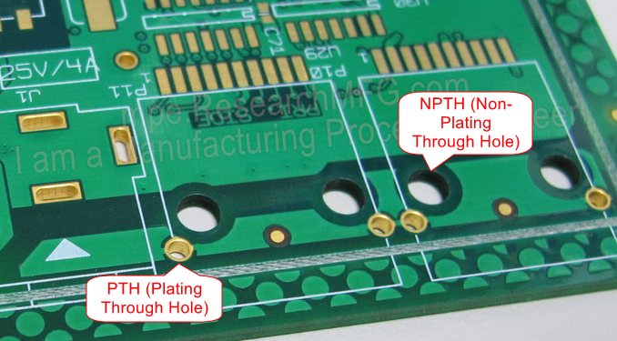
PTH Characteristics
- Conductive Interior: The entire inner surface of a PTH is coated with conductive material, visible as a shiny metallic surface.
- Connection Pads: PTHs typically have connection pads (annular rings) on both outer layers and any internal layers they pass through.
- Smaller Final Diameter: Because plating adds material to the hole walls, the finished hole diameter of a PTH is smaller than the initially drilled size (typically by twice the plating thickness).
- Solder Coverage: During assembly, solder typically wicks up into PTHs, creating visible fillets around component leads.
NPTH Characteristics
- Non-Conductive Interior: The hole walls show the base substrate material (usually FR-4) without metallic coating.
- Absence of Connection Pads: NPTHs may have no copper around them or only minimal keep-out areas, depending on their purpose.
- True to Drilled Size: Since no material is added to the hole walls, NPTHs maintain their original drilled diameter.
- No Solder Wicking: Solder generally doesn’t adhere to NPTH walls unless specifically required for mechanical bonding.
Electrical and Mechanical Properties
PTH Properties
- Electrical Conductivity: Excellent conductivity through the board thickness, with typical resistance in the milliohm range for standard sizes.
- Current Carrying Capacity: Can handle substantial current, with capacity increasing with larger diameters and thicker plating.
- Mechanical Strength: The plated copper adds structural reinforcement to the hole, making PTHs more resistant to mechanical stress.
- Thermal Transfer: Provides good thermal conductivity between layers, useful for heat dissipation.
- Impedance Characteristics: Affects high-frequency signal transmission due to parasitic capacitance and inductance.
NPTH Properties
- Electrical Isolation: Provides complete electrical isolation between layers unless intentionally bridged by other means.
- No Current Carrying Capacity: Cannot conduct electricity through the board thickness.
- Pure Mechanical Function: Serves only mechanical purposes without contributing to circuit functionality.
- Thermal Insulation: Offers minimal thermal transfer between layers compared to PTH.
- No Signal Integrity Impact: Doesn’t affect high-frequency signals unless in very close proximity to traces.
Applications and Use Cases
Typical PTH Applications
- Through-Hole Component Mounting: Traditional components with wire leads (resistors, capacitors, connectors) are inserted into PTHs and soldered.
- Via Connections: In multi-layer boards, PTHs (often called vias when small) connect traces between different layers.
- Power and Ground Connections: Large PTHs are used to distribute power and ground planes across layers.
- Heat Transfer Paths: Some designs use arrays of PTHs to transfer heat between layers to heatsinks or other cooling features.
- Test Points: PTHs can serve as access points for test probes during debugging and validation.
Common NPTH Applications
- Mechanical Mounting: Screw holes, standoff mounts, and other mechanical fasteners typically use NPTHs to prevent short circuits.
- Board Alignment: Tooling holes for manufacturing and assembly fixtures are always NPTH.
- Component Clearance: Some components require NPTHs to prevent unwanted electrical connections to internal planes.
- Ventilation and Drainage: NPTHs allow airflow or liquid drainage without creating electrical paths.
- High-Voltage Isolation: In high-voltage designs, NPTHs maintain proper creepage and clearance distances.
Design Considerations
PTH Design Factors
- Aspect Ratio: The ratio of hole depth to diameter affects plating quality. Standard PCBs maintain 8:1 or less, while advanced designs may go to 10:1.
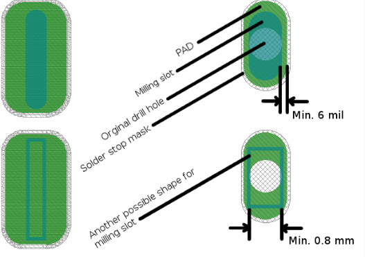
- Annular Ring: Sufficient copper around the hole (typically ≥5 mil) ensures reliable connections and prevents breakout.
- Thermal Relief: Connections to plane layers often use thermal relief patterns to prevent heat sinking during soldering.
- Via Types: Through-hole vias, blind vias, and buried vias offer different layer connection options.
- Signal Integrity: Stub length, antipads, and via shielding affect high-speed performance.
NPTH Design Factors
- Clearance: Adequate spacing from nearby copper features to prevent accidental contact.
- Tolerance: Often requires tighter positional tolerance than PTH for mechanical alignment.
- Solder Mask: May need solder mask dams to prevent solder wicking into holes during assembly.
- Board Strength: Large or closely spaced NPTHs can weaken the PCB structure.
- Plating Compatibility: Must be clearly specified to prevent accidental plating during fabrication.
Advantages and Limitations
PTH Advantages
- Layer Interconnectivity: Enables complex multi-layer designs.
- Mechanical Strength: Provides robust component mounting.
- Thermal Management: Aids in heat distribution.
- Reliability: Proven technology with well-understood failure modes.
- Repairability: Easier to rework than many surface mount connections.
PTH Limitations
- Higher Cost: Additional processing steps increase fabrication expense.
- Board Real Estate: Consume more space than surface mount alternatives.
- Frequency Limitations: Can degrade high-speed signal quality.
- Manufacturing Complexity: Requires precise process control.
- Thermal Stress: Differential expansion can cause reliability issues.
NPTH Advantages
- Lower Cost: Fewer processing steps reduce fabrication expense.
- Electrical Isolation: Prevents unwanted connections.
- Design Flexibility: Pure mechanical holes enable various mounting options.
- Manufacturing Simplicity: Easier to produce with fewer potential defects.
- High-Voltage Safety: Maintains proper isolation distances.
NPTH Limitations
- No Electrical Function: Cannot provide layer connections.
- Weaker Structure: Unplated holes are more prone to cracking under stress.
- Limited Applications: Only useful for specific mechanical purposes.
- Solder Issues: May require special processing to prevent solder wicking.
- Misuse Potential: Designers might accidentally use when PTH is needed.
Recent Developments and Future Trends
The electronics industry continues to evolve, impacting how PTHs and NPTHs are used in PCB design:
- High-Density Interconnect (HDI): Laser-drilled microvias are replacing some traditional PTHs in compact designs.
- Via-in-Pad: Placing vias directly in component pads saves space but requires careful plating.
- Conductive Hole Fill: Filled and capped vias provide planar surfaces for component mounting.
- Advanced Materials: New substrates with better thermal and mechanical properties affect hole reliability.
- Additive Manufacturing: 3D-printed electronics may revolutionize how through-holes are created.
Despite these advancements, the fundamental distinction between PTH and NPTH remains relevant, as each serves distinct purposes that continue to be essential in PCB functionality.

Conclusion
The choice between Plated Through-Holes (PTH) and Non-Plated Through-Holes (NPTH) in PCB design depends fundamentally on the required electrical and mechanical functionality. PTHs provide the critical electrical connections between layers that enable complex multi-layer circuits, while NPTHs serve important mechanical roles without affecting the board’s electrical characteristics.
Understanding their differences in manufacturing, structure, properties, and applications allows designers to make informed decisions that optimize both PCB performance and cost-effectiveness. As electronic devices continue to evolve toward higher densities and more specialized applications, the proper use of PTH and NPTH technologies remains a cornerstone of reliable PCB design and manufacturing.
By carefully considering the requirements of each hole in their designs—whether it needs to conduct electricity or simply provide mechanical support—engineers can create PCBs that meet increasingly demanding performance specifications while maintaining manufacturing efficiency and reliability.