The Evolution and Impact of PCB 3D Printers in Modern Electronics
Introduction
The world of electronics has undergone a significant transformation over the past few decades, with the advent of new technologies that have revolutionized the way we design, prototype, and manufacture electronic devices. One of the most groundbreaking innovations in recent years is the development of PCB (Printed Circuit Board) 3D printers. These devices have the potential to disrupt traditional manufacturing processes, enabling faster prototyping, reduced costs, and greater design flexibility. This article explores the evolution, functionality, benefits, and future prospects of PCB 3D printers, shedding light on their impact on the electronics industry.
1. The Evolution of PCB Manufacturing
Before delving into the specifics of PCB 3D printers, it is essential to understand the traditional methods of PCB manufacturing. Historically, PCBs have been produced using subtractive manufacturing techniques. This process involves etching away unwanted copper from a substrate to create the desired circuit pattern. While effective, this method is time-consuming, requires specialized equipment, and generates significant waste.
The need for more efficient and environmentally friendly manufacturing processes led to the exploration of additive manufacturing techniques, commonly known as 3D printing. Initially, 3D printing was primarily used for creating physical prototypes and models. However, as the technology advanced, it became clear that 3D printing could also be applied to the production of electronic components, including PCBs.
2. What is a PCB 3D Printer?
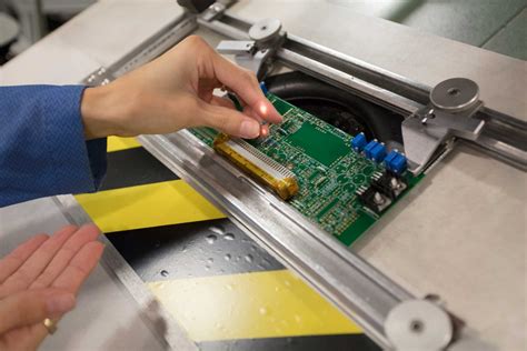
A PCB 3D printer is a specialized type of 3D printer designed to create printed circuit boards layer by layer using additive manufacturing techniques. Unlike traditional 3D printers that use plastic or metal filaments, PCB 3D printers utilize conductive and insulating materials to create the intricate patterns of a circuit board. These printers can produce multi-layer PCBs with complex geometries, making them ideal for prototyping and small-scale production.
3. How PCB 3D Printers Work
The operation of a PCB 3D printer can be broken down into several key steps:
3.1. Design and Preparation
The process begins with the creation of a digital design file, typically using CAD (Computer-Aided Design) software. This file contains the layout of the PCB, including the placement of components, traces, and vias. Once the design is finalized, it is converted into a format that the 3D printer can interpret, such as G-code.
3.2. Material Selection
PCB 3D printers use a combination of conductive and insulating materials to create the circuit board. Conductive materials, such as silver or copper nanoparticles, are used to form the electrical traces, while insulating materials, such as polymers, are used to create the substrate and separate the conductive layers.
3.3. Printing Process
The printing process involves depositing the conductive and insulating materials layer by layer onto a build platform. The printer follows the digital design file to create the precise patterns required for the PCB. Some PCB 3D printers use inkjet technology to deposit the materials, while others use extrusion-based methods similar to traditional 3D printers.
3.4. Curing and Post-Processing
Once the printing is complete, the PCB may undergo a curing process to solidify the materials and ensure proper adhesion between layers. Additional post-processing steps, such as drilling holes for through-hole components or applying a protective coating, may also be required.
4. Benefits of PCB 3D Printers
The adoption of PCB 3D printers offers several advantages over traditional manufacturing methods:
4.1. Rapid Prototyping
One of the most significant benefits of PCB 3D printers is the ability to quickly produce prototypes. Designers can iterate on their designs in a matter of hours, rather than waiting days or weeks for a traditional PCB to be manufactured. This accelerated prototyping process allows for faster development cycles and more efficient testing of new ideas.
4.2. Cost-Effectiveness
PCB 3D printers can significantly reduce the cost of producing small batches of PCBs. Traditional manufacturing methods often require expensive tooling and setup costs, which can be prohibitive for small-scale production. In contrast, 3D printing eliminates the need for tooling, making it a more cost-effective option for low-volume production runs.
4.3. Design Flexibility
3D printing enables greater design flexibility, allowing for the creation of complex geometries and multi-layer PCBs that would be difficult or impossible to achieve with traditional methods. Designers can experiment with unconventional shapes and layouts, leading to more innovative and optimized electronic devices.
4.4. Reduced Waste
Traditional PCB manufacturing generates a significant amount of waste, particularly during the etching process. PCB 3D printers, on the other hand, use only the materials needed to create the circuit board, resulting in minimal waste. This makes 3D printing a more environmentally friendly option.
4.5. On-Demand Production
PCB 3D printers enable on-demand production, allowing manufacturers to produce PCBs as needed without the need for large inventories. This can reduce storage costs and minimize the risk of obsolescence, particularly in industries where technology evolves rapidly.
5. Challenges and Limitations
While PCB 3D printers offer numerous benefits, there are also several challenges and limitations that need to be addressed:
5.1. Material Limitations
The materials used in PCB 3D printing are still relatively limited compared to those available for traditional PCB manufacturing. Conductive materials, in particular, may not offer the same level of conductivity as traditional copper traces, which can impact the performance of high-frequency or high-power circuits.
5.2. Resolution and Precision
The resolution and precision of PCB 3D printers are generally lower than those of traditional manufacturing methods. This can limit the complexity and density of the circuits that can be produced, particularly for fine-pitch components and high-density interconnects.
5.3. Speed
While PCB 3D printers are faster than traditional methods for prototyping, they may not be as efficient for large-scale production. The layer-by-layer printing process can be time-consuming, particularly for multi-layer PCBs with complex geometries.
5.4. Post-Processing Requirements
PCB 3D printers often require additional post-processing steps, such as curing, drilling, and coating, which can add time and complexity to the manufacturing process. These steps may also require specialized equipment and expertise.
6. Future Prospects
Despite these challenges, the future of PCB 3D printing looks promising. Advances in materials science, printing technology, and software are likely to address many of the current limitations, making PCB 3D printers more versatile and capable.
6.1. Improved Materials
Research is ongoing to develop new conductive and insulating materials that offer better performance and compatibility with 3D printing. For example, advancements in nanoparticle-based inks could lead to conductive traces with higher conductivity and improved adhesion to substrates.
6.2. Enhanced Resolution and Precision
Improvements in printing technology, such as higher-resolution print heads and more precise deposition methods, could enable the production of finer and more complex circuits. This would open up new possibilities for high-density interconnects and advanced electronic devices.
6.3. Integration with Other Technologies
PCB 3D printers could be integrated with other manufacturing technologies, such as pick-and-place machines for component assembly, to create a more streamlined and automated production process. This would further reduce the time and cost associated with producing electronic devices.
6.4. Wider Adoption
As the technology matures and becomes more accessible, PCB 3D printers are likely to see wider adoption across various industries. From consumer electronics to aerospace and medical devices, the ability to rapidly prototype and produce custom PCBs on-demand will drive innovation and competitiveness.
Conclusion
PCB 3D printers represent a significant leap forward in the field of electronics manufacturing. By enabling rapid prototyping, reducing costs, and offering greater design flexibility, these devices have the potential to transform the way we create and produce electronic devices. While there are still challenges to overcome, ongoing advancements in materials, technology, and software are likely to address these limitations, paving the way for a future where PCB 3D printing is a standard tool in the electronics industry. As the technology continues to evolve, it will be exciting to see how PCB 3D printers shape the future of electronics and drive innovation in the years to come.


