The Evolution and Importance of Printed Circuit Boards (PCBs) in Modern Computing
Introduction to PCBs
Printed Circuit Boards (PCBs) form the foundational infrastructure of virtually all modern electronic devices, serving as the central nervous system that connects and supports various electronic components. In the realm of computing, PCBs are particularly crucial, providing the platform upon which processors, memory chips, and other critical components are mounted and interconnected. From smartphones to supercomputers, PCBs enable the complex electrical pathways that make digital computation possible.
The development of PCB technology has paralleled and enabled the exponential growth of computing power described by Moore’s Law. As computers have become more powerful and compact, PCBs have evolved from simple single-layer boards to sophisticated multi-layered structures with microscopic traces and advanced materials. This article explores the technology behind computer PCBs, their manufacturing processes, design considerations, and future trends that will shape the next generation of computing hardware.
Historical Development of PCB Technology
The concept of printed wiring emerged in the early 20th century, with primitive versions appearing in gramophones and early radios. However, the modern PCB as we know it today was developed during World War II for military applications. The U.S. Army’s development of the proximity fuse required a reliable, mass-producible method for connecting electronic components, leading to the first true printed circuit boards.
In the computing realm, early computers like ENIAC (1945) used point-to-point wiring and later, wire wrap techniques. The transition to PCBs began in the 1950s as computers became more complex. IBM’s revolutionary System/360 mainframes in the 1960s utilized advanced multi-layer PCBs that set new standards for reliability and density.
The personal computer revolution of the 1980s drove PCB technology forward, with manufacturers developing techniques for higher component density and automated assembly. Today’s computer PCBs represent the culmination of nearly a century of continuous innovation in materials, manufacturing processes, and design methodologies.
Anatomy of a Computer PCB
A typical computer motherboard PCB is a marvel of engineering that integrates numerous subsystems into a cohesive whole. The base material, or substrate, is typically made from FR-4, a glass-reinforced epoxy laminate that provides mechanical stability and electrical insulation. High-performance computers may use specialized materials like polyimide or ceramic-filled laminates for better thermal and electrical properties.
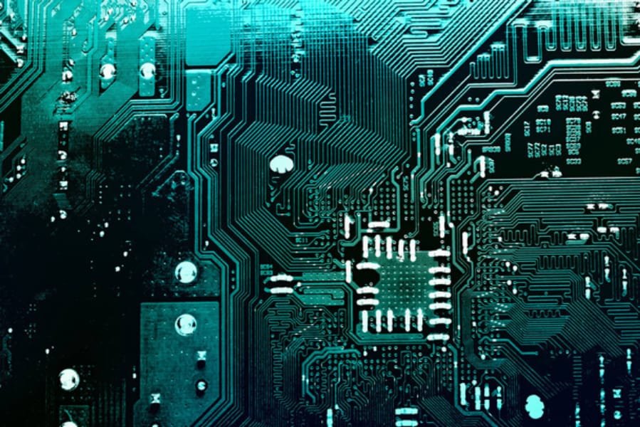
The conductive pathways, called traces, are typically made of copper and carry electrical signals between components. These traces are arranged in multiple layers (often 4 to 12 in modern computers) separated by insulating material. Vias—plated-through holes—connect traces between different layers, creating a three-dimensional network of interconnections.
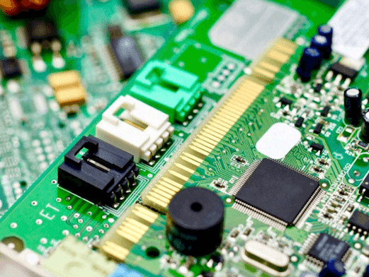
Key areas of a computer PCB include:
- CPU Socket/Area: The most densely routed section with thousands of connections to the processor
- Memory Slots: Carefully designed to maintain signal integrity for high-speed memory access
- Power Delivery Network: Multiple layers dedicated to distributing clean power throughout the board
- Expansion Slots: PCIe connectors for graphics cards and other peripherals
- Chipset and I/O Area: Hosting supporting chips and external connectors
PCB Manufacturing Process for Computer Applications
The production of high-quality computer PCBs involves numerous precise steps:
- Design and Layout: Using specialized EDA (Electronic Design Automation) software, engineers create the PCB layout according to electrical and mechanical requirements.
- Material Preparation: The base laminate is cleaned and prepared for patterning.
- Patterning: Photolithography transfers the circuit pattern onto the copper layers. This involves applying photoresist, exposing it to UV light through a mask, and developing the pattern.
- Etching: Chemical solutions remove unwanted copper, leaving only the desired traces.
- Lamination: For multi-layer boards, individual layers are aligned and bonded together under heat and pressure.
- Drilling: Precision drills create holes for vias and component leads. High-density interconnect (HDI) boards may use laser drilling for microvias.
- Plating: Copper is electroplated to form conductive vias and through-holes.
- Solder Mask Application: A protective coating is applied everywhere except component pads.
- Surface Finish: Coatings like HASL (Hot Air Solder Leveling), ENIG (Electroless Nickel Immersion Gold), or OSP (Organic Solderability Preservative) are applied to protect exposed copper and facilitate soldering.
- Silkscreen Printing: Component identifiers and other markings are added.
- Testing and Inspection: Automated optical inspection (AOI) and electrical testing verify board quality.
For computer motherboards, the process is particularly demanding due to the high layer count, fine features, and strict quality requirements. A typical motherboard might undergo hundreds of quality control checks during manufacturing.
Design Considerations for Computer PCBs
Designing PCBs for modern computers presents unique challenges that require careful consideration of numerous factors:
Signal Integrity
With processors operating at multi-gigahertz frequencies and memory buses transferring data at rates exceeding 50 GT/s (GigaTransfers per second), maintaining signal integrity is paramount. Designers must carefully control trace impedance, minimize crosstalk between signals, and manage signal reflections. Techniques like length matching (ensuring critical signals travel equal distances) and proper termination are essential.
Power Delivery
Modern CPUs can draw over 200 amps at low voltages, requiring sophisticated power delivery networks. This involves multiple power planes, careful capacitor placement, and sometimes even embedded voltage regulator modules (VRMs). Power integrity analysis ensures stable voltage levels despite rapidly changing current demands.
Thermal Management
High-performance components generate significant heat that must be dissipated. PCB designers incorporate thermal vias, heatsink mounting points, and sometimes even embedded heat pipes or vapor chambers in the board itself. The layout must consider airflow and thermal gradients across the board.
Electromagnetic Compatibility (EMC)
Computer PCBs must minimize electromagnetic interference (EMI) both to comply with regulations and prevent interference with onboard components. This involves careful grounding strategies, shielding, and sometimes EMI-absorbing materials.
Manufacturability and Cost
While pushing technological limits, designs must remain manufacturable at reasonable costs. This involves balancing layer count, material choices, and feature sizes against production capabilities and budget constraints.
Advanced PCB Technologies in Modern Computers
As computing demands increase, PCB technology continues to evolve with several advanced techniques now common in high-performance computers:
High-Density Interconnect (HDI)
HDI PCBs use finer traces (down to 2 mil or 50 μm), smaller vias (including microvias less than 100 μm in diameter), and higher connection pad density. This allows for more compact designs and better high-frequency performance.
Embedded Components
Some computer PCBs now incorporate passive components (resistors, capacitors) within the board layers, saving surface space and improving electrical performance by reducing parasitic inductance.
Flexible and Rigid-Flex PCBs
While not common in traditional desktop computers, these are increasingly used in laptops and mobile devices where space is at a premium. They allow three-dimensional packaging solutions that can conform to device shapes.

Advanced Materials
For extreme applications (high-end servers, aerospace computers), exotic materials like polyimide, PTFE, or ceramic-filled laminates offer better thermal stability and electrical properties than standard FR-4.
Optical Interconnects
Some experimental and high-performance computing PCBs incorporate optical waveguides alongside electrical traces, allowing for extremely high-bandwidth, low-latency communication between components.
Future Trends in Computer PCB Technology
As computing continues to advance, PCB technology must evolve to meet new challenges:
3D System Integration
Future computer PCBs may incorporate more three-dimensional packaging techniques, such as package-on-package (PoP) configurations, through-silicon vias (TSVs), and other advanced integration methods that blur the line between PCB and chip packaging.
Higher Frequency Operation
With processors moving into the millimeter-wave spectrum (30-300 GHz) for some applications, PCB materials and design techniques must adapt to maintain signal integrity at these extremely high frequencies.
Improved Thermal Management
As power densities increase, innovative cooling solutions will need to be integrated directly into PCB structures, possibly including microfluidic cooling channels or advanced thermal interface materials.
Sustainable Materials
Environmental concerns are driving development of biodegradable substrates, lead-free solders, and recycling-friendly designs that maintain performance while reducing ecological impact.
AI-Optimized Designs
Machine learning algorithms are increasingly being used to optimize PCB layouts, potentially discovering novel configurations that human designers might overlook, especially for complex, high-speed designs.
Conclusion
Printed Circuit Boards remain the unsung heroes of the computing revolution, providing the essential infrastructure that makes modern computation possible. From the simplest microcontrollers to the most powerful supercomputers, PCBs form the physical framework that brings electronic components together into functional systems.
As computing technology advances toward artificial intelligence, quantum computing, and beyond, PCB technology will continue to evolve to meet these new challenges. The future of computer PCBs likely holds three-dimensional architectures, optical-electrical hybrids, and materials science breakthroughs that we can scarcely imagine today.
Understanding PCB technology is crucial for anyone involved in computer hardware design, manufacturing, or repair. As the bridge between abstract computation and physical reality, PCBs will remain fundamental to computing for the foreseeable future, quietly enabling each new generation of technological progress.


