The Future of Electronics: Innovations in New Energy PCBs
Introduction to New Energy PCBs
Printed Circuit Boards (PCBs) have long been the backbone of electronic devices, but their role is becoming increasingly critical in the era of new energy technologies. New Energy PCBs represent a specialized category of circuit boards designed specifically for renewable energy systems, electric vehicles, energy storage solutions, and other clean technology applications. These advanced PCBs must meet exceptional standards of reliability, efficiency, and durability while operating in demanding environments.
The global shift toward sustainable energy solutions has created unprecedented demand for PCBs that can handle high power loads, resist extreme temperatures, and maintain performance over extended periods. From solar inverters to battery management systems in electric vehicles, New Energy PCBs are enabling the transition to a low-carbon future by providing the essential electronic infrastructure for green technologies.
This article explores the unique requirements, materials, design considerations, and manufacturing processes that distinguish New Energy PCBs from conventional circuit boards. We will examine their applications across various sectors of the renewable energy industry and consider future trends that will shape their development in the coming years.
Key Requirements for New Energy PCBs
New Energy PCBs face significantly different operational challenges compared to traditional electronic applications. These specialized circuit boards must be engineered to meet several critical requirements that are unique to renewable energy and clean technology systems.
High Power Handling Capacity is perhaps the most fundamental requirement. Unlike consumer electronics that typically operate at low voltages, new energy applications often involve hundreds of volts and substantial current flows. Solar inverters, for instance, must convert the DC output from photovoltaic panels (which can reach 600V or more for residential systems and 1500V for utility-scale installations) into grid-compatible AC power. This demands PCBs with robust current-carrying capacity, adequate creepage and clearance distances, and materials that can withstand high voltages without breakdown.
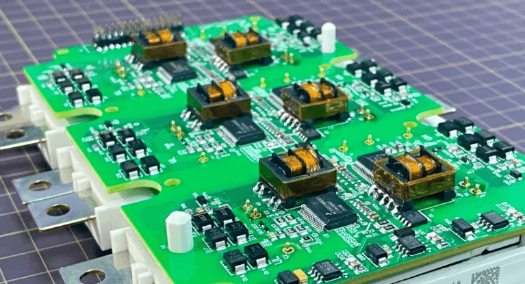
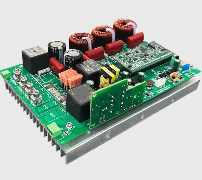
Thermal Management presents another major challenge. Power electronics in energy conversion systems generate considerable heat, and excessive temperatures can degrade performance or lead to premature failure. New Energy PCBs frequently incorporate thermal vias, metal cores (especially aluminum), or specialized substrates with high thermal conductivity to dissipate heat effectively. Some advanced designs even integrate liquid cooling channels directly into the PCB structure for high-power applications like electric vehicle drivetrains.
Environmental Durability is equally crucial. Many new energy systems operate in harsh conditions—solar installations endure UV exposure and wide temperature swings, wind turbine electronics face vibration and moisture, while electric vehicle components must withstand thermal cycling and mechanical stress. New Energy PCBs employ conformal coatings, robust substrate materials, and corrosion-resistant finishes to ensure long-term reliability in these challenging environments.
High Reliability and Long Service Life expectations further differentiate these PCBs. While consumer electronics might have a lifespan measured in years, energy infrastructure is expected to operate reliably for decades. Solar inverters typically carry 10-25 year warranties, requiring PCBs with exceptional longevity. This necessitates careful material selection, conservative design margins, and rigorous quality control during manufacturing.

Advanced Materials for New Energy Applications
The demanding requirements of new energy applications have driven the development and adoption of specialized PCB materials that go beyond the standard FR-4 used in conventional electronics. These advanced materials address the unique challenges of power density, thermal management, and environmental resistance.
Metal-Clad and Insulated Metal Substrates (IMS) have become increasingly prevalent, particularly in power conversion applications. Aluminum-based PCBs offer excellent thermal conductivity (typically 1-3 W/mK compared to 0.3 W/mK for FR-4), allowing heat to be efficiently transferred away from power components to heatsinks or enclosures. Copper-clad alternatives provide even better thermal performance (up to 400 W/mK for pure copper) for the most demanding applications. These metal-core boards often use a thermally conductive but electrically insulating dielectric layer (such as ceramic-filled polymers) to maintain electrical isolation while enabling heat transfer.
Ceramic Substrates represent another important material category, particularly for high-temperature or high-frequency applications. Aluminum oxide (Al₂O₃) and aluminum nitride (AlN) PCBs offer superior thermal conductivity (AlN can reach 170-200 W/mK) and can operate at temperatures exceeding 350°C. These properties make them ideal for concentrated photovoltaic systems, high-power LED arrays, and certain electric vehicle power modules. Direct Bonded Copper (DBC) ceramics, which feature copper foil bonded directly to both sides of a ceramic substrate, are particularly effective for high-power density designs.
High-Tg (Glass Transition Temperature) Materials are essential for applications subject to thermal cycling or sustained high temperatures. While standard FR-4 has a Tg around 130-140°C, specialized epoxy, polyimide, or PTFE-based materials can offer Tg values exceeding 170°C or even 250°C. These materials resist delamination and maintain mechanical stability under thermal stress, crucial for reliability in solar inverters that experience daily temperature fluctuations or electric vehicle components near heat sources.
High-Current Copper Weight is another critical material consideration. New Energy PCBs frequently employ thicker copper layers (2 oz/ft² to 20 oz/ft² or more) compared to the 0.5 oz/ft² to 2 oz/ft² typical in consumer electronics. The increased copper cross-section reduces resistive losses and improves current-carrying capacity, essential for power distribution in battery systems or high-current busbars integrated into the PCB structure.
Design Innovations for Energy Applications
The unique demands of new energy systems have spurred numerous innovations in PCB design methodology and layout techniques. These advancements optimize performance, reliability, and manufacturability while meeting the stringent requirements of power electronics and renewable energy applications.
High-Power Layout Techniques differ substantially from conventional digital or low-power analog design. New Energy PCBs must carefully manage current density to prevent localized heating and voltage drops. This often involves using polygon pours instead of thin traces for high-current paths, implementing symmetrical layouts to balance current distribution, and incorporating multiple vias in parallel when transitioning layers to minimize resistance. Thermal relief connections become critical to manage heat dissipation while maintaining solderability during assembly.
Embedded Components represent a significant design innovation, particularly for space-constrained applications like electric vehicles. By embedding passive components (resistors, capacitors) within the PCB layers or placing power devices in cavities with direct thermal paths to heatsinks, designers can reduce overall system size, improve thermal performance, and enhance reliability by eliminating solder joints that might fail under thermal cycling. Some advanced designs even incorporate planar magnetics (transformers, inductors) directly into the PCB layers for power conversion applications.
High-Voltage Design Considerations require special attention to clearance and creepage distances to prevent arcing or leakage currents. New Energy PCBs often incorporate slotting or groove cutouts in the board to increase surface distance between high-voltage nodes, use specialized conformal coatings to mitigate contamination risks, and may implement guard rings or other field-shaping techniques to manage electric field distribution. The layout must also consider the dielectric properties of the substrate material at operating voltages.
EMI/RFI Mitigation Strategies are crucial in power electronics, where fast switching of high currents can generate significant electromagnetic interference. Careful placement of noisy and sensitive circuits, proper grounding schemes, and the strategic use of shielding layers all contribute to meeting electromagnetic compatibility requirements. Some designs incorporate integrated shielding cans or ferrite-loaded materials directly into the PCB structure to contain interference.
Flex-Rigid and 3D Packaging Solutions are increasingly employed to meet the complex interconnection requirements of modern energy systems while saving space and weight. Electric vehicle battery management systems, for example, often use flex-rigid designs to connect multiple modules while withstanding vibration. Three-dimensional packaging approaches, including stacked or folded PCB assemblies, help optimize the use of available space in compact energy storage or power conversion units.
Manufacturing Challenges and Solutions
The production of New Energy PCBs presents unique manufacturing challenges that require specialized processes, equipment, and quality control measures. These challenges stem from the combination of advanced materials, high-power requirements, and stringent reliability expectations characteristic of clean energy applications.
Thick-Copper Processing poses several manufacturing difficulties. Laminating and patterning PCBs with copper weights above 3 oz/ft² requires modified etching processes to achieve proper trace definition without undercutting. Laser direct imaging (LDI) systems often replace traditional photolithography for improved accuracy with thick copper layers. Plated through-holes must accommodate higher currents, necessitating thicker copper plating in vias (frequently 25-50 μm compared to 15-25 μm for standard boards) and potentially filled vias for enhanced thermal and electrical performance.
Thermal Management Feature Fabrication demands precision manufacturing techniques. Creating effective thermal vias—which are often arrayed in large numbers beneath power components—requires careful drilling and plating to ensure consistent quality across the board. Metal-core boards introduce additional processing steps like routing or punching the metal substrate, which must be performed without damaging the delicate dielectric layer. Some advanced designs incorporate complex embedded heat pipes or liquid cooling channels that push the boundaries of conventional PCB manufacturing.
High-Voltage Testing and Inspection becomes more critical and challenging as operating voltages increase. Automated optical inspection (AOI) systems must be calibrated to detect subtle defects that could lead to partial discharge or breakdown at high potentials. Specialized testing equipment capable of applying and measuring high voltages (up to several kV for some applications) is required to verify dielectric strength and surface insulation resistance. These tests often need to be performed under environmental stress (elevated temperature and humidity) to ensure robust performance in field conditions.
Material Handling and Processing of advanced substrates requires adjustments throughout the manufacturing workflow. Ceramic and metal-clad boards may need specialized drilling equipment (laser or diamond-coated drills) and modified lamination cycles. High-Tg materials often require higher pressing temperatures and longer cure times during lamination. The thermal expansion mismatches between different materials in multilayer constructions must be carefully managed to prevent warping or delamination during processing.
Quality Control and Traceability requirements are typically more rigorous than for conventional PCBs, reflecting the critical nature of many new energy applications. Many manufacturers implement enhanced documentation systems that track material lots, process parameters, and test results for every board. Some automotive and energy sector customers require full manufacturing process certification (such as IATF 16949 for automotive) and may mandate statistical process control (SPC) for key parameters. These measures help ensure the long-term reliability expected from energy infrastructure components.

Applications in Renewable Energy Systems
New Energy PCBs find diverse applications across the spectrum of renewable energy generation, storage, and distribution systems. Each application presents unique challenges that drive continuous innovation in PCB technology.
Solar Power Systems rely heavily on advanced PCBs at multiple points in the energy conversion chain. Photovoltaic (PV) combiner boxes use PCBs to aggregate outputs from multiple solar panels while providing overcurrent protection and monitoring. Maximum Power Point Tracking (MPPT) controllers employ sophisticated PCB designs to optimize energy harvest from PV arrays under varying light conditions. Solar inverters—which convert DC from panels to grid-compatible AC—contain power stages with high-current PCBs, gate driver circuits, and control electronics, all requiring careful thermal management and high-voltage isolation.
Wind Turbine Electronics present challenges of vibration, moisture, and wide temperature ranges. PCBs in wind applications include pitch control systems (managing blade angle), power converters for variable-speed generators, and condition monitoring equipment. These often employ ruggedized designs with conformal coatings, mechanical reinforcement, and components rated for extended temperature ranges. Offshore wind farms present particularly harsh environments, driving the need for corrosion-resistant materials and enhanced protection against salt spray and humidity.
Energy Storage Systems for both grid-scale and residential applications depend on sophisticated PCB technology. Battery Management Systems (BMS) require precise voltage and temperature monitoring across numerous battery cells, with some designs incorporating distributed PCB modules that connect to each cell or module. These PCBs must provide excellent signal integrity for accurate measurements while withstanding the electrical noise environment of high-power battery packs. Power conversion systems for energy storage similarly demand robust PCBs capable of handling bidirectional power flow with high efficiency.
Electric Vehicle Components represent one of the fastest-growing applications for New Energy PCBs. Beyond the BMS mentioned earlier, EV power electronics include DC-DC converters (stepping between battery voltage and accessory system voltages), onboard chargers, and the critical traction inverter that drives the motor. These systems push PCB technology to its limits, requiring designs that combine high power density, exceptional thermal performance, and resistance to vibration and thermal cycling. The automotive industry’s quality and reliability standards add further constraints to the design and manufacturing process.
Smart Grid Infrastructure increasingly incorporates advanced PCBs for power monitoring, switching, and communication. Solid-state transformers, flexible AC transmission system (FACTS) devices, and grid-edge controllers all rely on power electronics implemented with specialized PCBs. These applications often require combinations of high-voltage and high-speed digital circuitry on the same board, presenting unique layout and isolation challenges.
Future Trends in New Energy PCB Technology
As renewable energy systems evolve and proliferate, PCB technology must continue advancing to meet emerging requirements. Several key trends are shaping the future development of New Energy PCBs across materials, design methodologies, and manufacturing processes.
Wide Bandgap Semiconductor Integration is driving significant changes in PCB requirements. The adoption of silicon carbide (SiC) and gallium nitride (GaN) power devices enables higher switching frequencies and operating temperatures than traditional silicon-based components. While this improves system efficiency and power density, it places greater demands on PCB materials to handle increased thermal loads and maintain signal integrity at higher frequencies. Future New Energy PCBs will need to accommodate these devices with low-loss dielectric materials, improved thermal interfaces, and layouts optimized for high-frequency power conversion.
Additive Manufacturing Techniques are beginning to transform PCB production, particularly for prototyping and low-volume specialized applications. Printed electronics technologies could enable direct deposition of conductive traces on unconventional substrates, potentially creating conformal PCBs that match the shape of their enclosure or heat sink. For high-power applications, 3D printing of thermal management features like heat pipes or cooling channels directly into the PCB structure may become practical. These approaches could significantly reduce lead times and enable more optimized geometries for thermal and electrical performance.
Integrated Sensor Networks are becoming increasingly important for condition monitoring and predictive maintenance in energy systems. Future New Energy PCBs may incorporate distributed temperature, humidity, vibration, and gas sensors directly into the board structure, enabled by printed or embedded sensor technologies. This would allow real-time monitoring of PCB health and early detection of potential failure modes, particularly valuable in remote or critical applications like offshore wind farms or grid infrastructure.
Advanced Thermal Management Solutions will continue to evolve to address rising power densities. We can expect to see wider adoption of vapor chamber technology integrated into PCBs, as well as more sophisticated liquid cooling solutions that may include microfluidic channels or phase-change materials. Thermally conductive but electrically insulating materials with higher performance than current options (such as boron nitride composites or advanced thermal interface materials) may enable new approaches to heat dissipation in power electronics.
Sustainability in PCB Manufacturing will grow in importance as the renewable energy sector seeks to minimize its own environmental impact. This may drive adoption of halogen-free materials, lead-free finishes compatible with high-reliability applications, and recycling-friendly designs that facilitate material recovery at end-of-life. Bio-based substrate materials and reduced chemical usage in manufacturing processes could further improve the environmental profile of New Energy PCBs.
AI-Optimized Designs may revolutionize how New Energy PCBs are laid out. Machine learning algorithms could explore vast design spaces to identify layouts that simultaneously optimize electrical performance, thermal management, and manufacturability—considerations that often involve complex trade-offs in conventional design processes. This could lead to novel PCB architectures specifically tailored to the unique requirements of energy conversion systems.
As these trends converge, New Energy PCBs will become increasingly sophisticated, enabling more efficient, reliable, and compact renewable energy systems. The ongoing evolution of PCB technology will play a crucial role in supporting the global transition to sustainable energy infrastructure across generation, storage, and distribution applications.
Conclusion
New Energy PCBs represent a critical enabling technology for the global transition to renewable energy and electrified transportation. These specialized circuit boards bridge the gap between conventional electronics and the demanding requirements of power conversion, energy storage, and clean energy generation systems. By addressing unique challenges in high-power handling, thermal management, and environmental durability, New Energy PCBs form the electronic foundation for solar inverters, wind turbine controls, electric vehicle power systems, and grid infrastructure.
The continued advancement of PCB materials, design methodologies, and manufacturing processes will directly contribute to improvements in renewable energy system efficiency, reliability, and cost-effectiveness. As wide bandgap semiconductors, additive manufacturing, and AI-driven design tools mature, they will enable new generations of New Energy PCBs capable of supporting even more ambitious clean energy deployments.
Looking ahead, the importance of New Energy PCBs will only grow as societies worldwide accelerate their decarbonization efforts. The innovations emerging in this specialized field of electronics manufacturing will play a vital role in achieving climate goals while meeting the world’s expanding energy needs. For engineers, researchers, and manufacturers, New Energy PCBs present both significant challenges and extraordinary opportunities to contribute to a more sustainable technological future.