The Impact of 5G Applications on the PCB Industry Chain
Abstract
The advent of 5G technology has brought revolutionary changes across multiple industries, and the Printed Circuit Board (PCB) sector is no exception. As a critical component in electronic devices, PCBs are facing new challenges and opportunities due to the increasing demands of 5G applications. This paper explores how 5G technology impacts the PCB industry chain, including material requirements, design complexity, manufacturing processes, and market dynamics. Additionally, it discusses the potential future trends and strategic adjustments that PCB manufacturers must consider to remain competitive in the 5G era.
1. Introduction
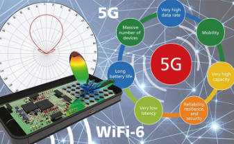
The fifth-generation (5G) wireless technology promises ultra-high-speed data transmission, low latency, and massive connectivity, enabling advancements in the Internet of Things (IoT), autonomous vehicles, smart cities, and industrial automation. However, these advancements impose stringent requirements on the underlying hardware, particularly PCBs, which serve as the backbone of electronic circuits.
The PCB industry must adapt to support higher frequencies, improved thermal management, and increased reliability. This paper examines the key areas where 5G applications are reshaping the PCB supply chain and analyzes the resulting challenges and opportunities.
2. Key Impacts of 5G on the PCB Industry
2.1 Increased Demand for High-Frequency and High-Speed PCBs
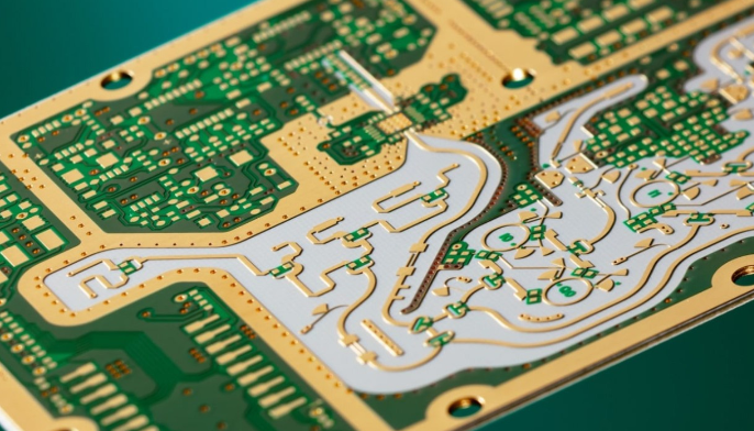
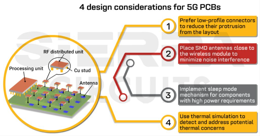
5G networks operate at higher frequencies (mmWave bands up to 100 GHz), necessitating PCBs with superior signal integrity and minimal loss. Traditional FR-4 materials are insufficient for these applications, leading to a shift toward high-frequency laminates such as PTFE (Teflon), Rogers, and ceramic-filled substrates.
- Material Innovations: PCB manufacturers must adopt low-loss dielectric materials to minimize signal attenuation.
- Design Complexity: High-speed PCBs require precise impedance control, advanced routing techniques, and reduced crosstalk.
2.2 Miniaturization and High-Density Interconnect (HDI) PCBs
5G devices, such as smartphones and base stations, demand compact yet high-performance PCBs. This trend drives the adoption of HDI technology, which enables finer traces, microvias, and multilayer stacking.
- Advanced Manufacturing Techniques: Laser drilling and sequential lamination are essential for producing HDI PCBs.
- Increased Layer Count: 5G infrastructure PCBs often require 20+ layers to accommodate complex circuitry.
2.3 Thermal Management Challenges
Higher power dissipation in 5G devices leads to increased heat generation. Effective thermal management becomes crucial to ensure reliability.
- Metal Core PCBs (MCPCBs): Used in power amplifiers and RF modules for better heat dissipation.
- Thermal Vias and Heat Sinks: Incorporated into designs to enhance cooling.
2.4 Rigid-Flex and Flexible PCBs for Wearables and IoT
5G enables more connected devices, including wearables and IoT sensors, which often require flexible PCBs for space-saving and durability.
- Adoption of Polyimide Substrates: Flexible PCBs benefit from bendable materials that withstand repeated flexing.
- Integration Challenges: Ensuring reliability in dynamic bending environments.
2.5 Supply Chain and Cost Pressures
The shift to advanced materials and processes increases production costs. Additionally, geopolitical factors (e.g., U.S.-China trade tensions) affect the PCB supply chain.
- Localized Manufacturing: Some companies are reshoring production to reduce dependency on global suppliers.
- Cost-Effective Alternatives: Research into cheaper high-performance materials is ongoing.
3. Market Opportunities and Industry Responses
3.1 Growth in 5G Infrastructure PCBs
The rollout of 5G base stations and small cells creates massive demand for high-frequency PCBs. Key players like AT&S, TTM Technologies, and Shennan Circuits are expanding production capacities.
3.2 Automotive and Industrial Applications
5G-enabled vehicles (V2X communication) and smart factories rely on robust PCBs with enhanced reliability.
3.3 Collaboration with Semiconductor Companies
PCB manufacturers must work closely with chipmakers to optimize packaging solutions, such as System-in-Package (SiP) and fan-out wafer-level packaging (FOWLP).
4. Future Trends and Strategic Recommendations
4.1 AI and Automation in PCB Manufacturing
AI-driven defect detection and automated assembly lines will improve yield rates and reduce costs.
4.2 Sustainable Manufacturing Practices
The PCB industry must address environmental concerns by adopting lead-free soldering and recyclable materials.
4.3 Investment in R&D for Next-Gen PCBs
Research into embedded components, additive manufacturing (3D-printed PCBs), and advanced substrates will be critical.
5. Conclusion
The 5G revolution is transforming the PCB industry, driving innovations in materials, design, and manufacturing. While challenges such as higher costs and technical complexities exist, the opportunities for growth in telecommunications, automotive, and IoT sectors are immense. PCB manufacturers must embrace technological advancements, optimize supply chains, and invest in R&D to thrive in the 5G era.
By adapting proactively, the PCB industry can not only withstand the disruptions brought by 5G but also emerge as a key enabler of next-generation electronics.