The Impact of Common Pads on PCB Soldering Quality
Abstract
This paper examines the effects of common (shared) pads on printed circuit board (PCB) soldering processes and final product quality. As electronic devices continue to shrink in size while increasing in complexity, the use of shared pads has become more prevalent in PCB design. While offering space-saving benefits, common pads introduce several challenges to the soldering process that can affect reliability, yield rates, and long-term performance. This article analyzes the various impacts including thermal management issues, solder bridging risks, inspection difficulties, and rework complications. The discussion includes design recommendations to mitigate these problems while still achieving space efficiency.
Introduction
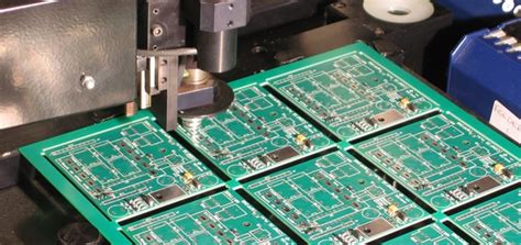
Modern PCB design frequently employs common pad configurations where multiple components share a single conductive land pattern. This practice has become particularly common in high-density interconnect (HDI) boards and miniaturized consumer electronics. While shared pads conserve valuable board space and can simplify routing, they present unique challenges during the soldering process that can compromise joint quality and reliability.
The soldering process—whether wave, reflow, or hand soldering—must accommodate the thermal and physical requirements of all components sharing the pad. When these requirements conflict or when process parameters aren’t optimized for the shared configuration, various soldering defects can occur. This paper systematically examines these potential issues and provides practical solutions for manufacturing professionals.

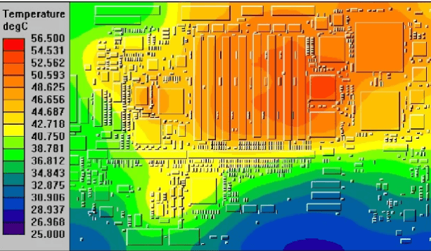
Thermal Management Challenges
Differential Heat Requirements
Components sharing a common pad often have different thermal mass and heat tolerance characteristics. For example, a pad shared between a small passive component and a large IC will experience uneven heat distribution during reflow. The smaller component may reach proper soldering temperature while the larger one remains underheated, or conversely, the larger component’s requirements may cause overheating of the smaller one.
Thermal Shadow Effects
In wave soldering, taller components can create thermal shadows that prevent proper solder flow to adjacent smaller components on the shared pad. This often results in incomplete fillets or cold solder joints on the shadowed components.
Solution Strategies:
- Staggered pad design: Create sub-pads within the common pad with thermal relief variations
- Selective soldering: Use different temperature zones or subsequent soldering processes
- Thermal mass balancing: Add thermal relief patterns or thermal ties to equalize heat distribution
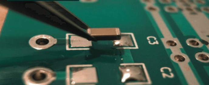
Solder Bridging Risks
Increased Occurrence Probability
Common pads inherently place component terminations in closer proximity, dramatically increasing the likelihood of solder bridges forming between them. This risk is particularly acute in fine-pitch components and when using lead-free solders with poorer wetting characteristics.
Solder Volume Management
Determining the appropriate solder volume for a shared pad is complex—insufficient solder creates dry joints while excess solder promotes bridging. The problem compounds when components have different solder volume requirements.
Mitigation Approaches:
- Solder mask defined (SMD) pads: Use solder mask to precisely control solderable areas
- Stepped stencil designs: Apply different solder paste volumes to different pad sections
- Component orientation: Arrange components to maximize spacing between terminations
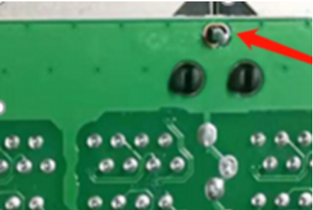
Inspection and Quality Control Difficulties
Optical Inspection Limitations
Automated optical inspection (AOI) systems struggle with shared pads because the expected solder joint appearance varies significantly across the pad area. Traditional inspection algorithms may flag acceptable joints as defective or miss real defects.
X-ray Inspection Challenges
Even with x-ray inspection, the overlapping features of multiple components can obscure view of solder joints, making void detection and fillet evaluation difficult.
Improved Inspection Methods:
- Custom inspection algorithms: Program AOI systems with shared-pad-specific criteria
- Multi-angle x-ray: Utilize tomographic techniques to separate overlapping features
- Enhanced test points: Add dedicated test points for critical shared pad connections
Rework and Repair Complications
Selective Desoldering Difficulties
Removing a single component from a shared pad without disturbing others is extremely challenging. The heat required for one component often remelts joints on adjacent components.
Solder Cleanup Issues
After component removal, cleaning excess solder from the shared pad without creating opens in remaining joints requires exceptional skill and often specialized tools.
Rework Strategies:
- Localized heating tools: Use micro hot air nozzles or thermal tweezers
- Solder dams: Incorporate solder mask barriers between components
- Sacrificial thermal mass: Add temporary heat sinks to protect adjacent components
Reliability Concerns
Stress Concentration Points
Shared pads often become stress concentration points during thermal cycling and mechanical shock. The differing coefficients of thermal expansion (CTE) between components can create shear forces that fatigue solder joints.
Current Carrying Capacity
Multiple components sharing current through a single pad may exceed the current capacity designed for a single connection point, leading to premature failure.
Reliability Enhancements:
- Reinforced pad structures: Use anchored or plugged vias within pads
- Stress relief geometries: Incorporate curved traces instead of right angles
- Current monitoring: Verify shared pad current loads during design
Design Recommendations
Layout Guidelines
- Maintain at least 0.2mm clearance between component terminations on shared pads
- Orient components to maximize spacing between solderable surfaces
- Avoid mixing component types (e.g., passives with ICs) on shared pads when possible
Pad Geometry Optimization
- Use teardrop or dog-bone pad shapes to improve solder flow control
- Consider partitioned pads with solder mask barriers for critical connections
- Implement micro-vias within pads for improved thermal and electrical performance
Process Adjustments
- Develop custom solder paste stencils for shared pad configurations
- Adjust reflow profiles to account for mixed thermal requirements
- Implement post-solder inspection protocols specific to shared pad joints
Conclusion
While common pads offer significant space-saving advantages in PCB design, they introduce multiple challenges to the soldering process that can affect manufacturing yield and product reliability. By understanding these impacts—thermal management issues, bridging risks, inspection difficulties, and rework complications—designers and process engineers can implement mitigation strategies. Careful pad design, process optimization, and specialized inspection techniques can maintain the benefits of shared pads while minimizing their drawbacks. As component densities continue to increase, the industry must develop even more sophisticated solutions for reliable shared pad implementation.
Future research directions should focus on advanced materials with self-limiting solder flow properties, smarter soldering processes with real-time thermal adaptation, and improved inspection technologies using machine learning for shared pad evaluation. By addressing these challenges, the electronics industry can continue its trend toward miniaturization without compromising soldering quality.