The Impact of Fiberglass Weave on PCB Performance: Understanding the Fiberglass Effect
Introduction to Fiberglass Effect in PCB Design
Printed Circuit Board (PCB) design has evolved significantly over the past decades, with increasing attention paid to the subtle material characteristics that affect signal integrity. Among these, the fiberglass effect—also known as the fiber weave effect or glass weave effect—has emerged as a critical consideration for high-speed digital designs. This phenomenon refers to the variations in dielectric properties caused by the uneven distribution of fiberglass and resin in the PCB substrate, which can lead to unexpected signal integrity issues, particularly in high-frequency applications.
The fiberglass effect gained prominence as signal rise times decreased below 1 nanosecond and data rates exceeded 1 Gbps. At these speeds, the microscopic structure of the PCB substrate begins to influence signal propagation in ways that were negligible at lower frequencies. Modern designs operating at multi-gigabit data rates (10Gbps, 25Gbps, and beyond) must account for these material variations to ensure consistent performance across all signal paths.
The Composition of PCB Substrates and Fiber Weave Patterns
Basic Structure of PCB Laminates
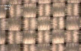
Most conventional PCBs use FR-4 (Flame Retardant 4) material, which consists of woven fiberglass cloth impregnated with epoxy resin. The fiberglass cloth provides mechanical strength, while the resin acts as the dielectric medium. This composite structure creates inherent inhomogeneity in the substrate’s electrical properties because the dielectric constant (Dk or εr) and dissipation factor (Df) differ between the fiberglass bundles and the resin-rich areas.
Common Weave Styles and Their Characteristics
Fiberglass cloth comes in several standard weave styles, each with distinct patterns that affect PCB performance differently:
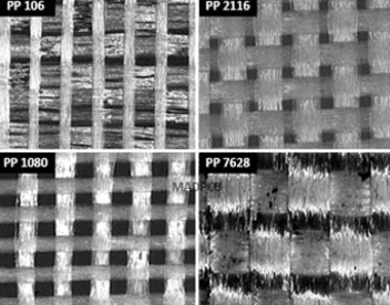
- 1080 Weave: One of the tightest weaves with approximately 60×47 threads per inch. The thin strands (about 2.5 mils wide) create relatively small periodic variations but with high density.
- 2116 Weave: A common choice with about 60×58 threads per inch and wider strands (about 4 mils). This creates more pronounced periodic variations than 1080 but with lower density.
- 7628 Weave: A much looser weave with about 44×32 threads per inch and very wide strands (about 9 mils). This creates significant periodic variations but with large resin-rich areas between bundles.
The selection of weave style involves trade-offs between mechanical properties (like dimensional stability) and electrical performance. Tighter weaves (like 1080) generally produce less pronounced fiberglass effects but may not provide sufficient mechanical strength for thicker boards.
Mechanism of the Fiberglass Effect
Dielectric Constant Variation
The fundamental cause of the fiberglass effect lies in the difference in dielectric constant between the fiberglass bundles (εr ≈ 6.0-6.4) and the resin regions (εr ≈ 3.0-3.4). As signals propagate through the PCB dielectric, they encounter alternating zones of high and low dielectric constant corresponding to the fiberglass weave pattern. These variations cause:
- Impedance Fluctuations: The local characteristic impedance of transmission lines varies with the instantaneous dielectric constant beneath the trace.
- Propagation Velocity Changes: Signal propagation speed varies as it moves through different dielectric regions (v = c/√εr).
- Phase Distortion: Different frequency components experience varying delays, leading to signal integrity issues.
Impact on Signal Integrity
The periodic nature of these dielectric variations creates several observable effects:
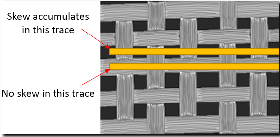
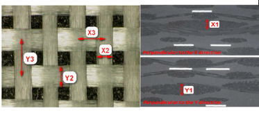
- Intra-Pair Skew: In differential pairs, if the two traces happen to align differently relative to the weave pattern, they may experience different propagation delays, leading to skew.
- Insertion Loss Variations: The inconsistent dielectric properties cause frequency-dependent loss characteristics that don’t follow smooth curves.
- Resonant Effects: At certain frequencies, the periodic structure can create standing wave patterns that exacerbate signal degradation.
- Jitter Generation: The uneven propagation characteristics can contribute to timing jitter in high-speed serial links.
Measurement and Characterization of Fiberglass Effects
Laboratory Observations
Advanced measurement techniques have revealed the concrete impact of fiberglass weave:
- Time Domain Reflectometry (TDR): Shows impedance variations along the length of a trace corresponding to the weave pattern.
- Vector Network Analyzer (VNA) Measurements: Reveal periodic variations in insertion loss and phase response.
- Microscopic Cross-Section Analysis: Correlates electrical measurements with physical weave structure.
Quantifying the Effect
Key parameters for characterizing fiberglass effect include:
- Dielectric Contrast Ratio (DCR): The ratio between fiberglass and resin dielectric constants (typically about 2:1 in FR-4).
- Spatial Periodicity: The distance between repeating weave patterns (typically 10-20 mils depending on weave style).
- Effective Dielectric Constant: The composite value that would produce equivalent electrical length.
Mitigation Strategies in PCB Design
Material Selection Approaches
- Spread Glass Weaves: Some manufacturers offer specialized materials with spread or randomized fiber distributions to reduce periodicity.
- Low-Dk Glass Styles: Using glass fibers with dielectric constants closer to the resin (e.g., NE-glass with εr ≈ 4.9).
- Non-Woven Substrates: Materials like Rogers’ hydrocarbon ceramics eliminate the weave effect entirely but at higher cost.
Design Techniques
- Trace Angle Optimization: Routing traces at 15°-30° angles to the weave pattern helps average out dielectric variations.
- Layer Stackup Planning: Placing critical high-speed layers adjacent to homogeneous core materials rather than woven prepreg.
- Differential Pair Compensation: Intentional length tuning to counteract expected skew from weave effects.
- Trace Width Adjustment: Slightly wider traces help average over more of the periodic structure.
Manufacturing Considerations
- Material Consistency Control: Working with manufacturers to ensure consistent weave orientation across panels.
- Advanced Simulation: Using 3D EM field solvers that can model material inhomogeneities.
- Design for Manufacturing (DFM): Accounting for typical weave patterns used by your fabrication house.
Simulation and Modeling Approaches
Analytical Models
First-order approximations treat the substrate as a periodic structure and apply transmission line theory with varying dielectric properties. These models can predict:
- Effective Dielectric Constant: Using volumetric averaging methods.
- Impedance Variations: Based on local dielectric constant under the trace.
- Skew Estimation: For differential pairs based on their offset from the weave pattern.
Numerical Simulation Techniques
Advanced simulation methods provide more accurate predictions:
- Finite Element Method (FEM): Models the exact geometry of fiber bundles and resin pockets.
- Finite Difference Time Domain (FDTD): Captures wave propagation through the inhomogeneous medium.
- Hybrid Methods: Combine analytical approximations with numerical solutions for efficiency.
Practical Simulation Tips
- Unit Cell Approach: Modeling one repeating section of the weave pattern with periodic boundary conditions.
- Statistical Analysis: Running multiple simulations with varying trace positions relative to the weave.
- Correlation with Measurements: Validating models against actual test board results.
Case Studies and Practical Examples
High-Speed Serial Link Design
A 28Gbps SerDes link showed unexpected eye closure that correlated with the PCB’s 2116 weave pattern periodicity. By rotating the critical traces 22° and using a tighter 1080 weave, the design achieved 30% improvement in eye opening.
DDR4 Memory System
A DDR4 interface exhibited timing violations between byte lanes. Analysis revealed fiberglass-induced skew variations up to 0.8ps/inch between lanes. The solution involved intentional length matching that accounted for the expected weave-related delays.
RF Power Amplifier Design
A 5GHz power amplifier showed gain variations across production units. The root cause was traced to inconsistent fiber weave orientation affecting microstrip line phase lengths. Switching to a spread-glass material reduced unit-to-unit variation by 60%.
Future Trends and Advanced Solutions
Emerging Material Technologies
- Nanostructured Dielectrics: Materials with engineered dielectric properties at the nanoscale.
- Isotropic Composite Substrates: Homogeneous mixtures achieving uniform electrical properties.
- Liquid Crystal Polymer (LCP): Provides excellent high-frequency characteristics without weave effects.
Design Methodologies
- Machine Learning for Weave Prediction: Using AI to predict and compensate for local dielectric variations.
- 3D Printed Electronics: Potential for completely homogeneous dielectric structures.
- Chip-Embedded Solutions: Moving critical interconnects into the package to avoid PCB dielectric issues.
Conclusion
The fiberglass effect represents a fundamental challenge in high-speed PCB design that stems from the very nature of composite substrate materials. As data rates continue climbing into the 50+Gbps range and beyond, understanding and mitigating these subtle material effects becomes increasingly critical. Successful designs in this regime require close collaboration between material scientists, PCB manufacturers, and signal integrity engineers.
By combining appropriate material selection, thoughtful design strategies, and advanced simulation techniques, engineers can effectively manage fiberglass effects to produce robust, high-performance electronic systems. The ongoing development of new materials and design methodologies promises to further mitigate these challenges in future generations of PCB technology.
Ultimately, mastering the fiberglass effect represents another step in the electronics industry’s relentless pursuit of pushing performance boundaries while working within the constraints of practical materials and manufacturing processes. Those designers who develop expertise in these subtle material effects will gain a competitive advantage in developing reliable high-speed electronic systems.


