The Impact of PCB Vias on Signal Transmission
Abstract
Printed Circuit Board (PCB) vias are essential interconnects that enable routing between different layers in multilayer boards. While indispensable for modern high-density PCB designs, vias introduce various effects that can significantly impact signal integrity. This paper examines the electrical characteristics of vias, their influence on signal transmission, and methods to mitigate adverse effects. Key considerations include impedance discontinuities, signal reflections, insertion loss, crosstalk, and their relationship with via geometry and materials. Practical design techniques are presented to optimize via performance in high-speed digital and high-frequency analog applications.
1. Introduction
1.1 The Role of Vias in PCBs
Vias serve as vertical interconnects that electrically connect different conductive layers in multilayer PCBs, enabling complex routing in limited board space. As electronic devices continue shrinking in size while increasing in functionality and speed, via design has become critical for maintaining signal integrity.
1.2 Importance of Via Analysis
With signal frequencies exceeding several gigahertz in modern electronics, vias that were once considered benign now significantly affect system performance. Understanding via effects allows designers to:
- Maintain signal integrity
- Control electromagnetic interference
- Minimize power delivery network impedance
- Achieve reliable high-speed data transmission
2. Electrical Characteristics of Vias
2.1 Equivalent Circuit Model
A via can be modeled as a complex impedance network consisting of:
- Inductance (L): Primarily from the via barrel (typically 0.1-1nH)
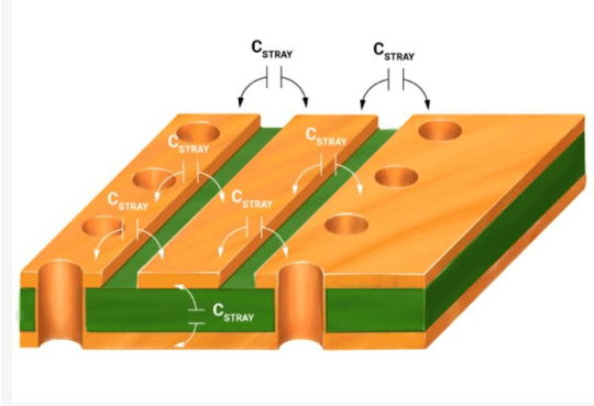
- Capacitance (C): Between the via pad and reference planes (typically 0.1-0.5pF)
- Resistance (R): DC resistance of the conductive material
- Conductance (G): Dielectric losses
The simplified lumped-element model for a via is shown in Figure 1.
[Figure 1: Equivalent circuit model of a via]
2.2 Impedance Discontinuity
Vias create impedance discontinuities due to:
- Changes in transmission line geometry
- Additional capacitive loading from pads
- Inductive effects of the barrel
- Anti-pad clearance in reference planes
The impedance mismatch causes signal reflections quantified by the reflection coefficient (Γ):
Γ = (Z_via – Z_line)/(Z_via + Z_line)
Where Z_via is the via’s characteristic impedance and Z_line is the transmission line impedance.
3. Signal Integrity Effects
3.1 Signal Reflections
Impedance discontinuities cause partial signal reflections that:
- Degrade signal quality
- Create ringing and overshoot
- Reduce timing margins
- Cause intersymbol interference (ISI)
The reflection magnitude depends on the frequency and the degree of impedance mismatch.
3.2 Insertion Loss
Vias introduce frequency-dependent attenuation from:
- Dielectric losses: Proportional to frequency
- Conductor losses: Increase with √f due to skin effect
- Radiation losses: Become significant at very high frequencies
The total insertion loss (IL) in dB can be expressed as:
IL = 20log10|S21|
Where S21 is the forward transmission coefficient.
3.3 Phase Distortion
The reactive components in vias cause non-linear phase response, leading to:
- Group delay variation
- Signal distortion
- Jitter in high-speed digital systems
3.4 Crosstalk
Unwanted coupling between adjacent vias can occur through:
- Capacitive coupling between via barrels
- Inductive coupling via shared return paths
- Electromagnetic radiation
Crosstalk increases with:
- Decreasing via spacing
- Increasing signal edge rates
- Longer via stubs
4. Via Structure and Performance Factors
4.1 Geometric Parameters
Key via dimensions affecting performance:
- Diameter: Larger diameters reduce inductance but increase capacitance
- Pad size: Larger pads increase capacitance
- Anti-pad size: Clearance in reference planes affects capacitance
- Barrel length: Proportional to inductance
- Stub length: Unused portion of via below signal layer
4.2 Material Properties
- Dielectric constant (Dk): Affects capacitance and propagation velocity
- Loss tangent (Df): Determines dielectric losses
- Conductor roughness: Impacts high-frequency resistance
- Plating quality: Affects conductivity and skin effect
4.3 Via Types and Their Characteristics
Different via structures exhibit varying signal integrity performance:
- Through-hole vias:
- Span entire board thickness
- Highest inductance
- Significant stub effects
- Blind vias:
- Connect outer layer to inner layer(s)
- Reduced stub length
- Lower inductance than through-hole
- Buried vias:
- Connect only inner layers
- No stubs
- Most complex manufacturing
- Microvias:
- Small diameter (<100μm)
- Typically laser-drilled
- Lowest inductance
- Used in HDI designs
5. Mitigation Techniques
5.1 Via Optimization Methods
- Stub removal:
- Back-drilling
- Laser ablation
- Using blind/buried vias
- Impedance matching:
- Controlled anti-pad sizing
- Via fencing
- Return path vias
- Crosstalk reduction:
- Increased via spacing
- Ground shielding vias
- Orthogonal routing
5.2 Advanced Via Structures
- Via-in-pad:
- Minimizes loop area
- Reduces inductance
- Requires careful plating
- Tented vias:
- Covered with solder mask
- Prevents solder wicking
- May affect high-frequency performance
- Filled vias:
- Conductive or non-conductive fill
- Improves thermal performance
- May change electrical characteristics
5.3 Design Guidelines
- High-speed signals:
- Minimize via count
- Use shortest possible vias
- Provide continuous return paths
- Differential pairs:
- Maintain symmetry
- Equalize via structures
- Use ground vias between pairs
- Power delivery:
- Multiple parallel vias
- Low-inductance configurations
- Proper decoupling
6. Simulation and Measurement
6.1 Modeling Approaches
- 3D EM simulation:
- HFSS, CST Microwave Studio
- Most accurate
- Computationally intensive
- 2.5D simulation:
- SIwave, Q2D
- Faster than 3D
- Limited geometry complexity
- Analytical models:
- Fast calculations
- Limited accuracy
- Useful for initial estimates
6.2 Measurement Techniques
- Time Domain Reflectometry (TDR):
- Characterizes impedance profile
- Identifies discontinuities
- Vector Network Analysis (VNA):
- Measures S-parameters
- Provides frequency response
- Eye diagram analysis:
- Evaluates system-level impact
- Assesses timing and noise margins
7. Case Studies
7.1 High-Speed Digital Application
A 10Gbps SerDes link analysis showing:
- Via stub effects on eye closure
- Improvement with back-drilling
- Optimal via placement
7.2 RF/Microwave Design
A 28GHz mmWave circuit demonstrating:
- Via coupling in antenna arrays
- Ground via shielding effectiveness
- Millimeter-wave via transitions
8. Future Trends
- Higher frequency challenges:
- THz applications
- Advanced materials
- Novel via structures
- 3D integration:
- Through-silicon vias (TSVs)
- Interposer technologies
- Heterogeneous integration
- Manufacturing advances:
- Smaller via sizes
- Improved plating techniques
- Additive manufacturing
9. Conclusion
PCB vias significantly impact signal transmission through various mechanisms including impedance discontinuities, reflections, loss, and crosstalk. These effects become increasingly critical as signal speeds continue rising. Careful via design incorporating proper geometry selection, return path management, and advanced mitigation techniques is essential for maintaining signal integrity in modern high-speed designs. Future technological developments will require continued innovation in via design and analysis methodologies to meet the demands of next-generation electronic systems.