The Impact of Poor PCB Design on Printing Processes
Abstract
Printed Circuit Board (PCB) design plays a crucial role in determining the success of the manufacturing process, particularly in printing and etching stages. Poor PCB design can lead to various defects, increased production costs, and reduced reliability of the final product. This paper examines the key aspects of PCB design that negatively affect printing processes, including solder mask application, silkscreen legibility, pad and trace integrity, and alignment issues. By understanding these challenges, designers can optimize their layouts to improve manufacturability and yield.
1. Introduction
The PCB manufacturing process involves multiple stages, including printing, etching, drilling, and plating. Among these, the printing process—particularly solder mask and silkscreen application—is highly sensitive to design flaws. Poorly designed PCBs can cause misalignment, ink bleeding, insufficient coverage, and other defects that impact both functionality and aesthetics.
This paper explores common PCB design mistakes and their effects on printing processes, providing recommendations to mitigate these issues.
2. Key PCB Design Flaws Affecting Printing Processes
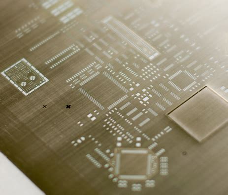
2.1 Improper Solder Mask Clearance
The solder mask is a protective layer applied over copper traces to prevent oxidation and short circuits. Poor design choices, such as insufficient solder mask clearance between pads and traces, can lead to:
- Solder Mask Bridging: When the mask spreads between closely spaced pads, causing unintended insulation and solderability issues.
- Incomplete Coverage: If openings are too small, the mask may not fully cover traces, exposing them to environmental damage.
- Mask Peeling: Poor adhesion due to incorrect expansion settings can cause the mask to peel during thermal cycling.
Recommendation: Follow manufacturer Design for Manufacturability (DFM) guidelines for minimum solder mask clearance (typically 0.05mm–0.1mm beyond pads).
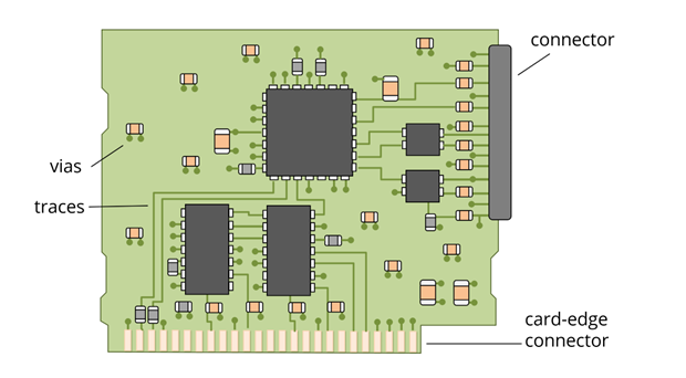
2.2 Incorrect Silkscreen Design
Silkscreen printing provides component labels, polarity markings, and logos. Poor silkscreen design can result in:
- Blurred or Unreadable Text: Text that is too small (below 0.8mm height) or too thin (below 0.15mm line width) may become illegible.
- Ink Bleeding: Overlapping silkscreen on pads or vias causes smudging and poor aesthetics.
- Misalignment: Text placed too close to component pads may shift during printing, leading to assembly errors.
Recommendation: Use a minimum font height of 1.0mm, avoid placing silkscreen over pads/vias, and maintain a 0.2mm clearance from solderable areas.
2.3 Poor Pad and Trace Geometry
The shape and size of pads and traces influence solder paste application and mask alignment:
- Inconsistent Pad Sizes: Non-standard pad dimensions can cause uneven solder paste deposition, leading to tombstoning or poor solder joints.
- Sharp Trace Corners: Acute angles in traces may trap etching chemicals or cause ink accumulation during printing.
- Insufficient Thermal Relief: Poor thermal relief design in ground/power planes can lead to uneven heating during reflow, affecting solder mask adhesion.
Recommendation: Use rounded corners for traces, standardized pad sizes, and proper thermal relief connections.
2.4 Inadequate Registration Tolerances
PCB printing relies on precise alignment between layers (copper, mask, silkscreen). Poor registration design can cause:
- Misaligned Solder Mask Openings: Mask misalignment exposes copper or covers pads, leading to soldering defects.
- Silkscreen Shift: Text may overlap with components, reducing readability.
Recommendation: Include fiducial marks and ensure sufficient tolerance margins (≥0.1mm) for layer alignment.
2.5 Incorrect Panelization Design
For mass production, PCBs are often panelized. Poor panel design affects printing uniformity:
- Insufficient Spacing Between Boards: Tight spacing can cause solder mask or silkscreen bleeding across boards.
- Improper Breakaway Tab Design: Weak tab designs may lead to cracking during depaneling, damaging printed layers.
Recommendation: Maintain at least 2mm spacing between boards and use robust breakaway tabs with rounded edges.
3. Case Studies
3.1 Case 1: Solder Mask Peeling Due to Poor Thermal Relief
A manufacturer reported frequent solder mask peeling on a high-power PCB. Analysis revealed insufficient thermal relief connections in ground planes, causing uneven heat distribution during curing. Redesigning the thermal reliefs resolved the issue.
3.2 Case 2: Silkscreen Misalignment in High-Density Designs
A compact IoT device suffered from illegible silkscreen due to text being placed too close to components. Increasing the font size and clearance improved readability without affecting functionality.
4. Conclusion
Poor PCB design significantly impacts printing processes, leading to defects that compromise quality and reliability. By adhering to DFM guidelines—optimizing solder mask clearance, silkscreen legibility, pad geometry, and registration tolerances—designers can enhance manufacturability and reduce production failures. Collaboration between designers and manufacturers is essential to identify and mitigate potential printing issues early in the design phase.