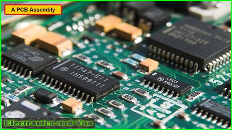
The Impact of Vias on High-Speed Signal Transmission in PCBs
Abstract
This paper examines the critical role of vias in printed circuit boards (PCBs) and their significant impact on high-speed signal transmission. As electronic devices continue to operate at higher frequencies and faster data rates, the design and implementation of vias have become increasingly important for maintaining signal integrity. The discussion covers the electrical characteristics of vias, their effects on signal quality, and various mitigation strategies to minimize negative impacts in high-speed designs.
1. Introduction
In modern PCB design, vias serve as essential conductive pathways connecting different layers of multilayer boards. While they provide necessary interlayer connections, vias introduce discontinuities in transmission lines that can significantly degrade signal quality at high frequencies. As data rates exceed several gigabits per second and clock frequencies move into the microwave range, the impact of vias on signal integrity becomes non-negligible.
This paper explores the electromagnetic behavior of vias, their equivalent circuit models, and the resulting effects on high-speed signals. We also present design techniques to optimize via performance in high-speed applications.
2. Electrical Characteristics of Vias
2.1 Physical Structure
A typical via consists of three main components:
- The barrel (conductive cylinder forming the interconnection between layers)
- The pad (annular ring connecting the barrel to traces)
- The anti-pad (clearance in reference planes around the via)
2.2 Equivalent Circuit Model
At high frequencies, vias exhibit complex impedance characteristics that can be modeled using lumped circuit elements:
- Inductance (L): Primarily from the via barrel, typically 0.1-1.0 nH depending on dimensions
- Capacitance (C): Between the via barrel and reference planes, typically 0.1-0.5 pF
- Resistance (R): DC resistance of the conductive material and skin effect at high frequencies
- Conductance (G): Dielectric losses in the surrounding material
The impedance discontinuity created by this combination of L and C elements causes signal reflections and degrades signal integrity.
3. Effects on High-Speed Signal Transmission
3.1 Signal Reflection
Impedance mismatches at via transitions create signal reflections characterized by:
- Reflection coefficient: Γ = (Zvia – Z0)/(Zvia + Z0)
- Where Zvia is the via’s characteristic impedance and Z0 is the transmission line impedance
These reflections cause:
- Ringing on signal edges
- Reduced signal amplitude
- Increased bit error rates in digital systems
3.2 Insertion Loss
Vias introduce frequency-dependent attenuation:
- Conductor losses from skin effect and surface roughness
- Dielectric losses in PCB material
- Radiation losses at high frequencies
The insertion loss typically follows the form:
IL(f) = α√f + βf + γf²
Where α, β, and γ represent different loss mechanisms.
3.3 Crosstalk
Unoptimized via arrangements can create:
- Capacitive coupling between adjacent vias
- Inductive coupling through shared return paths
- Electromagnetic radiation between via stubs
3.4 Mode Conversion
Differential signals experience:
- Common-mode conversion due to asymmetrical via structures
- Increased electromagnetic interference (EMI)
- Degraded differential signal quality
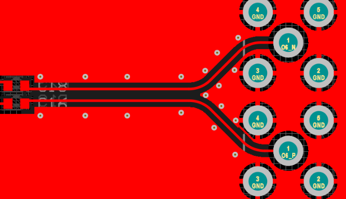
4. Key Factors Affecting Via Performance
4.1 Geometrical Parameters
- Diameter: Smaller diameters reduce capacitance but increase inductance
- Aspect ratio: Height/diameter ratio affects impedance characteristics
- Pad size: Larger pads increase parasitic capacitance
- Anti-pad size: Affects capacitance to reference planes
4.2 Material Properties
- Dielectric constant (Dk) of PCB material
- Loss tangent (Df) affecting high-frequency losses
- Conductivity of via plating material
4.3 Stackup Design
- Distance to reference planes
- Number of layer transitions
- Via stub length (unused portion of via barrel)
4.4 Layout Considerations
- Via spacing and arrangement
- Return current path continuity
- Proximity to other vias and components
5. Mitigation Techniques
5.1 Via Optimization
- Controlled impedance vias: Matching via impedance to transmission lines
- Via back-drilling: Removing unused via stubs
- Microvias: Smaller diameter vias for high-density interconnects
5.2 Return Path Management
- Providing adjacent ground vias for signal transitions
- Maintaining continuous reference planes
- Using stitching capacitors for layer transitions
5.3 Differential Via Design
- Maintaining symmetry in differential pairs
- Minimizing length mismatch
- Implementing via shielding techniques
5.4 Advanced Via Structures
- Buried vias: Connecting only internal layers
- Blind vias: Connecting outer to inner layers
- Via-in-pad: Direct component connection to vias
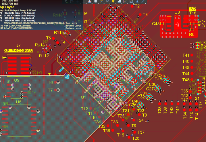
6. Simulation and Measurement
Modern design workflows incorporate:
- 3D electromagnetic field solvers for accurate via modeling
- Time-domain reflectometry (TDR) for impedance characterization
- Vector network analyzer (VNA) measurements for S-parameter extraction
These tools enable designers to:
- Predict via performance before fabrication
- Optimize via structures for specific applications
- Validate designs through measurement correlation

7. Case Studies
7.1 10 Gbps Serial Link
Analysis of via effects on eye diagram:
- Without optimization: 30% eye closure
- With optimized vias: <10% eye closure
7.2 28 GHz mmWave Design
Via stub effects on insertion loss:
- 2 mm stub: 3 dB loss at 28 GHz
- Back-drilled stub: <0.5 dB loss
7.3 DDR4 Memory Interface
Impact of via arrangements on signal skew:
- Conventional layout: 15 ps skew
- Optimized layout: <5 ps skew
8. Future Trends
Emerging technologies addressing via challenges:
- Terahertz via structures: For beyond 100 GHz applications
- 3D integrated vias: For heterogeneous integration
- Optical vias: For optical-electrical PCB interconnects
9. Conclusion
Vias present significant challenges for high-speed signal transmission in modern PCBs, introducing impedance discontinuities, signal reflections, and various loss mechanisms. However, through careful design, optimization, and advanced manufacturing techniques, these effects can be mitigated to acceptable levels. As data rates continue to increase, the importance of proper via design will only grow, requiring designers to pay close attention to via characteristics and their impact on overall system performance.
Future PCB designs will need to incorporate more sophisticated via structures and simulation methodologies to maintain signal integrity at ever-higher frequencies while meeting the demands for miniaturization and increased functionality.