The Importance and Methodology of ICT Testing in Modern Electronics Manufacturing
Introduction
In the rapidly evolving field of electronics manufacturing, ensuring the quality and reliability of printed circuit boards (PCBs) and assembled products is critical. In-Circuit Testing (ICT) is one of the most widely used methods for verifying the functionality and integrity of electronic components at the production stage. This article explores the fundamentals of ICT testing, its advantages, methodologies, challenges, and future trends in the industry.
1. What is ICT Testing?
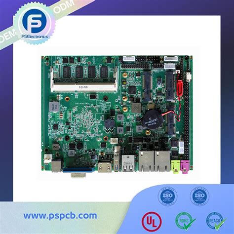
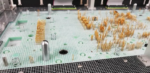
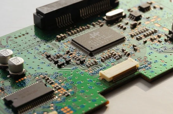
In-Circuit Testing (ICT) is an automated testing technique used to validate the electrical performance of individual components on a PCB. It involves using a bed-of-nails fixture or flying probe tester to make direct contact with test points on the board, allowing for precise measurements of resistance, capacitance, voltage, and other electrical parameters.
Key Objectives of ICT Testing
- Verify the presence, orientation, and correct values of components (resistors, capacitors, ICs, etc.).
- Detect manufacturing defects such as shorts, opens, missing components, or incorrect placements.
- Ensure proper soldering connections.
- Validate analog and digital circuit functionality before final assembly.
2. Types of ICT Testing
ICT testing can be categorized into different approaches depending on the complexity and requirements of the PCB assembly:
A. Static ICT (Analog Testing)
- Measures passive components (resistors, capacitors, inductors).
- Checks for continuity and isolation between circuits.
- Identifies solder bridges or open circuits.
B. Dynamic ICT (Digital Testing)
- Tests active components (ICs, microcontrollers, FPGAs).
- Verifies logic states, signal integrity, and communication protocols.
- May involve boundary scan (JTAG) testing for complex digital circuits.
C. Flying Probe ICT
- Uses movable probes instead of a fixed bed-of-nails fixture.
- Ideal for low-volume or prototype testing due to flexibility.
- Slower than traditional ICT but requires no custom fixtures.
D. Combination ICT and Functional Testing
- Some systems integrate ICT with functional testing to validate both component-level and system-level performance.
3. Advantages of ICT Testing
ICT offers several benefits in electronics manufacturing:
A. High Fault Coverage
- Detects up to 95% of manufacturing defects, including solder defects, wrong components, and incorrect placements.
B. Fast and Automated
- Tests can be completed in seconds, making it suitable for high-volume production.
C. Early Defect Detection
- Identifies issues before final assembly, reducing rework costs.
D. Repeatable and Reliable
- Automated test procedures eliminate human error.
E. Cost-Effective for Mass Production
- While initial fixture costs are high, per-unit testing costs are low for large batches.
4. ICT Testing Methodology
The ICT process follows a structured approach:
A. Test Program Development
- Engineers create a test program based on the PCB design files (Gerber, BOM, schematics).
- Test points are selected for optimal coverage.
B. Fixture Design
- A bed-of-nails fixture is designed to align with PCB test points.
- Spring-loaded pins ensure reliable electrical contact.
C. Test Execution
- Power-off Tests: Continuity, isolation, and passive component checks.
- Power-on Tests: Voltage, current, and digital signal validation.
- Boundary Scan (if applicable): Tests digital IC interconnects.
D. Data Analysis and Reporting
- Test results are logged, and defective boards are flagged for repair.
- Statistical process control (SPC) helps track manufacturing trends.
5. Challenges in ICT Testing
Despite its advantages, ICT testing has some limitations:
A. High Initial Cost
- Custom fixtures and test development require significant investment.
B. Limited Access in High-Density PCBs
- Miniaturization and complex layouts reduce test point accessibility.
C. Difficulty Testing Some Components
- High-frequency, RF, and some analog circuits may require additional testing methods.
D. Not a Replacement for Functional Testing
- ICT verifies individual components but does not fully validate system behavior.
6. Future Trends in ICT Testing
As electronics become more advanced, ICT testing is evolving with new technologies:
A. Integration with AI and Machine Learning
- Predictive analytics can optimize test coverage and reduce false failures.
B. Increased Use of Flying Probe Testers
- Improved speed and accuracy make them viable for more applications.
C. IoT and Smart Manufacturing
- Real-time monitoring and adaptive test strategies enhance efficiency.
D. 3D ICT for Complex Assemblies
- Advanced probing techniques for multi-layer and flexible PCBs.
Conclusion
ICT testing remains a cornerstone of PCB manufacturing, providing high fault detection rates and ensuring product reliability. While challenges such as fixture costs and high-density PCB limitations exist, advancements in automation, AI, and flexible probing techniques are expanding its capabilities. As electronics continue to evolve, ICT testing will adapt to meet the demands of next-generation devices, maintaining its critical role in quality assurance.
By leveraging ICT alongside other testing methods (such as AOI and functional testing), manufacturers can achieve optimal production efficiency and deliver defect-free products to the market.