The Manufacturing Process Flow of PCB Inner Layers
Introduction
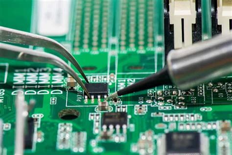
Printed Circuit Boards (PCBs) are essential components in modern electronics, providing mechanical support and electrical connections for electronic components. The inner layers of multi-layer PCBs play a critical role in ensuring signal integrity, power distribution, and overall board reliability. The manufacturing process of PCB inner layers involves several precise steps, including material preparation, imaging, etching, and inspection. This article provides a detailed overview of the inner layer fabrication process, highlighting key techniques and quality control measures.
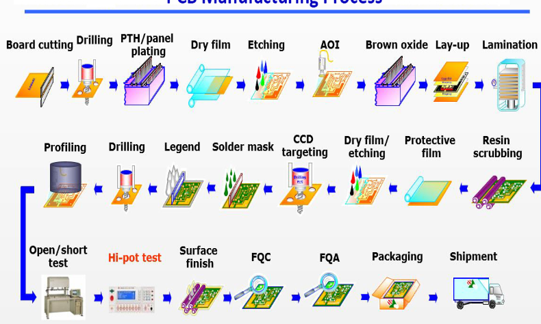
1. Material Preparation
The first step in manufacturing PCB inner layers is selecting and preparing the base material. The most commonly used substrate is FR-4, a glass-reinforced epoxy laminate with good mechanical and electrical properties.
Key Steps:
- Copper Clad Laminate (CCL) Selection: The core material consists of a dielectric layer (usually epoxy resin with fiberglass) laminated with thin copper foil (typically 0.5 oz to 2 oz in thickness).
- Cutting: Large panels are cut into smaller workable sizes based on the PCB design requirements.
- Surface Cleaning: The copper surface is cleaned to remove oxidation, dust, and contaminants using chemical or mechanical methods to ensure proper adhesion of the photoresist.
2. Inner Layer Imaging (Photolithography)
The imaging process transfers the circuit pattern from the design files onto the copper-clad laminate.
Key Steps:
- Photoresist Application: A light-sensitive photoresist (either liquid or dry film) is applied to the copper surface. Dry film photoresist (DFR) is commonly used due to its uniformity and ease of handling.
- Exposure: The panel is exposed to UV light through a photomask (film or glass) containing the circuit pattern. The exposed areas harden, while the unexposed areas remain soluble.
- Development: The board is immersed in a developer solution, which removes the unexposed photoresist, leaving behind the desired circuit pattern.
3. Etching
After imaging, the unwanted copper is removed through a chemical etching process.
Key Steps:
- Etching Solution: Typically, an alkaline ammonia-based or acidic cupric chloride solution is used to dissolve the exposed copper.
- Stripping: The remaining photoresist is stripped away using a sodium hydroxide (NaOH) or potassium hydroxide (KOH) solution, revealing the copper traces.
- Rinsing & Drying: The panel is thoroughly rinsed to remove chemical residues and then dried.
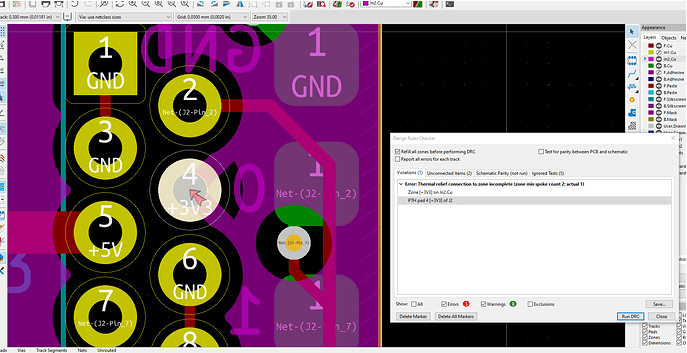
4. Automated Optical Inspection (AOI)
To ensure the inner layers meet design specifications, an Automated Optical Inspection (AOI) system scans the boards for defects such as shorts, opens, or incorrect trace widths.
Key Checks:
- Copper Trace Integrity: Verifies that all traces are correctly formed without breaks or excessive thinning.
- Alignment Accuracy: Ensures that the pattern matches the design files.
- Defect Marking: Any detected defects are marked for repair or rejection.
5. Oxide Treatment (Optional)
For multi-layer PCBs, an oxide treatment (also called brown oxide or black oxide) is applied to enhance adhesion between inner layers and prepreg (bonding material).
Key Steps:
- Micro-etching: A mild chemical etch roughens the copper surface to improve bonding.
- Oxide Coating: A controlled oxidation process forms a thin, porous oxide layer on the copper.
- Neutralization & Drying: The panel is neutralized to stop further oxidation and dried.
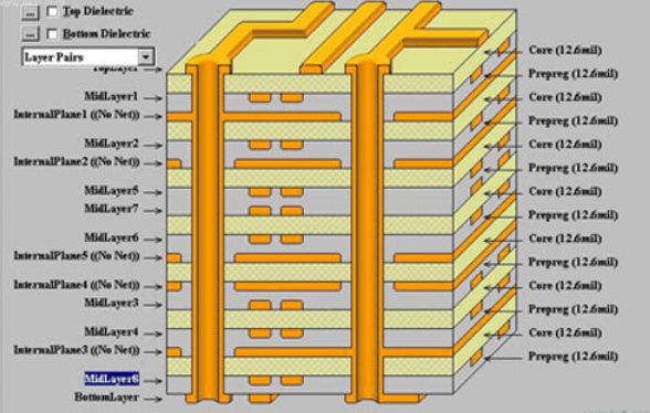
6. Lamination (for Multi-Layer PCBs)
After inner layer processing, multiple layers are stacked and laminated under heat and pressure to form a solid board.
Key Steps:
- Layer Stack-Up: Inner layers are aligned with prepreg (partially cured epoxy resin) and outer copper foils.
- Lamination Pressing: The stack is placed in a hydraulic press, where heat (typically 180°C–200°C) and pressure bond the layers together.
- Cooling & Trimming: The laminated panel is cooled and trimmed to remove excess material.

7. Post-Lamination Processing
Once laminated, the panel undergoes further processing, including drilling, plating, and outer layer patterning.
Conclusion
The manufacturing of PCB inner layers is a highly precise process involving material preparation, photolithography, etching, inspection, and surface treatment. Each step must be carefully controlled to ensure signal integrity, reliability, and performance in the final PCB. Advanced techniques such as laser direct imaging (LDI) and automated inspection continue to improve yield and quality in modern PCB fabrication.
By understanding these processes, engineers and manufacturers can optimize designs for better manufacturability and performance in complex multi-layer PCBs.