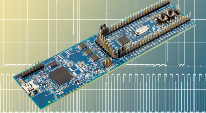
The method of PCB power design
As all electronics engineer must konw,PCB design plays a crucial role in design.Taking a power supply as an example ,pcb design directly impacts its EMC performance, output noise ,interference immunity,and even basic functionality .PCB routing in a power supply differs slightly differs slightly from other hardware.How should it be designed?
Spacing
For high voltage products,row spacing must be carefully considered.While spacing that meets safety requirements is ideal,in many cases,spacing is determined by experience with products that do not or cannot meet certification requirements .
What is the appropriate spacing width?Factors such as panel cleanliness,ambient humidity,and other contaminants must be considered.
For power supply inputs,even if the board material is guaranteed to be clean and sealed,a MOSFET drain near 600V Can be dangerous if the spacing is less than 1mm!
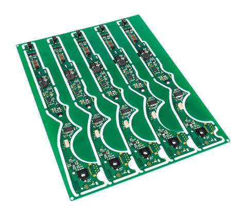
Components on the Board Edge
When placing chip capacitor or other sensitive components on a PCB,the orientation of the PCB divider must be considered.The figure shows several placement methods.The device requires a comparison of stress levels.
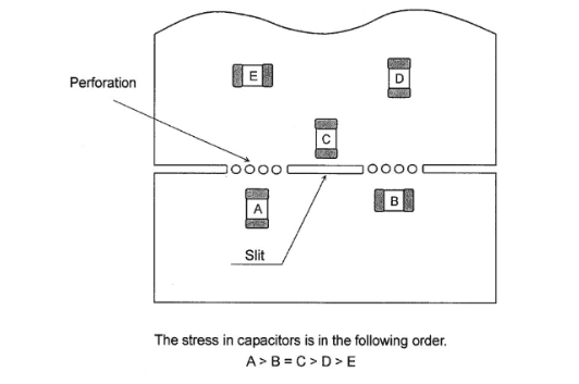
It can be seen that the device should be kept away from and parallel to the edge of the separator,otherwise,it may be damaged by the PCB separator.
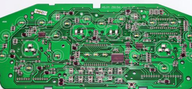
Loop Area
Whether input or output,power or signal loops,should be kept as small as possible.Power loops emit electromagnetic fields,which will result in poor EMI characteristics or excessive output noise,and may cause anomalies if received by the control loop.On the other hand,if the power loop area is large.on the other hand, if the power loop area is large ,the equivalent parasitic inductance increases, which may increase the peak leakage nosie.
Signal lines
For the entire control section,consider keeping it away from the power section.If the two are separated due to other constrains,control lines should not run parallel to power lines,otherwise it may cause abnormal operation and oscillation of the power supply.
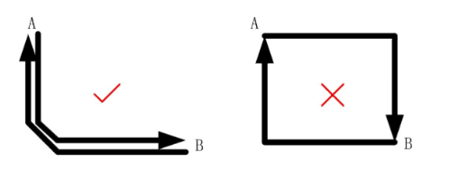
Also,if the control line is long,it should be placed close to the preceding and following pair of lines,or the two lines should be placed on opposite sides of the PCB,facing each other,to reduce the loop area and avoid electromagenetic filed interference from the power section.Figure 2 illustrates correct and incorrect signal wiring methods between two AHB points.
PCB Power Supply Design Methods
Copper Propagation
Sometimes,copper is completely unnecessary and should even be avoided.If the copper surface is large enough and its voltage is constantly changing.It can act as an antenna,radiating electromagnetic waves from the surrounding area.
On the other hand,it can easily pick up noise.Copper is generally only allowed at static node,such as the“floor”node at the ouput,to increse output capacitance and filter out some noise signals.