The Necessity of Copper Pour in PCB Design
Introduction
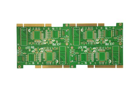
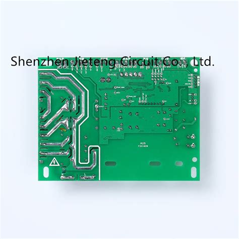
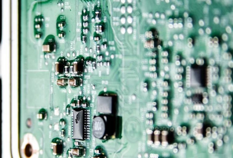
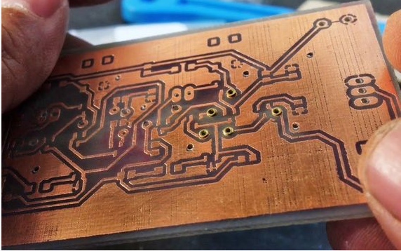
Printed Circuit Board (PCB) design is a critical aspect of electronic product development, influencing performance, reliability, and manufacturability. Among various design techniques, copper pour (also known as copper flooding or copper fill) is a widely used practice that involves filling unused areas of a PCB with solid or hatched copper. This technique offers multiple benefits, including improved signal integrity, thermal management, and electromagnetic compatibility (EMC). However, improper use of copper pour can also introduce challenges such as unintended capacitance, manufacturing defects, or signal interference.
This article explores the necessity of copper pour in PCB design, discussing its advantages, potential drawbacks, and best practices for implementation
1. Advantages of Copper Pour in PCB Design
1.1 Enhanced Signal Integrity and Reduced Noise
Copper pour plays a vital role in maintaining signal integrity by providing a low-impedance return path for high-frequency signals. Key benefits include:
- Ground Plane Functionality: A solid copper pour connected to the ground plane reduces loop inductance, minimizing electromagnetic interference (EMI) and crosstalk between traces.
- Shielding Effect: Copper pour acts as a shield, preventing noise coupling between adjacent signal traces, especially in mixed-signal designs.
- Controlled Impedance: In high-speed designs, copper pour helps maintain consistent impedance by reducing parasitic inductance and capacitance.
1.2 Improved Thermal Management
Electronic components generate heat during operation, and excessive temperatures can degrade performance or cause failure. Copper pour aids in thermal dissipation by:
- Distributing Heat Evenly: Large copper areas act as heat sinks, spreading thermal energy across the board.
- Enhancing Heat Transfer: Copper’s high thermal conductivity helps dissipate heat from power components (e.g., voltage regulators, power amplifiers).
- Supporting Thermal Vias: Copper pour can be used in conjunction with thermal vias to transfer heat to inner layers or the opposite side of the PCB.
1.3 Electromagnetic Compatibility (EMC) Benefits
EMC compliance is crucial for electronic devices to function without interfering with other systems. Copper pour contributes to EMC by:
- Reducing Radiated Emissions: A continuous ground plane minimizes loop areas, lowering EMI radiation.
- Preventing Ground Bounce: Proper copper distribution ensures a stable reference voltage, reducing ground noise in high-speed circuits.
- Shielding Sensitive Traces: Copper pour around high-frequency or analog signals prevents external interference.
1.4 Manufacturing and Mechanical Stability
Copper pour also impacts PCB fabrication and structural integrity:
- Reducing Etching Time: Large copper areas balance copper distribution, preventing uneven etching and warping during manufacturing.
- Enhancing Mechanical Strength: Copper reinforcement in flexible PCBs improves durability.
- Preventing Copper Thieving Issues: Uniform copper distribution avoids uneven plating in high-current designs.
2. Potential Challenges and Mitigation Strategies
Despite its advantages, improper copper pour implementation can lead to issues such as:
2.1 Increased Parasitic Capacitance
Excessive copper near high-speed signal traces can introduce unwanted capacitance, leading to signal degradation. Solution: Use hatched copper pour or adjust clearance rules to minimize parasitic effects.
2.2 Ground Loops and Short Circuits
Poorly designed copper pour can create unintended ground loops or short circuits. Solution:
- Ensure proper clearance between copper and non-ground nets.
- Use thermal relief connections for component pads to prevent soldering issues.
2.3 Manufacturing Defects
Uneven copper distribution may cause warping or etching inconsistencies. Solution:
- Balance copper coverage across layers.
- Follow manufacturer Design for Manufacturing (DFM) guidelines.
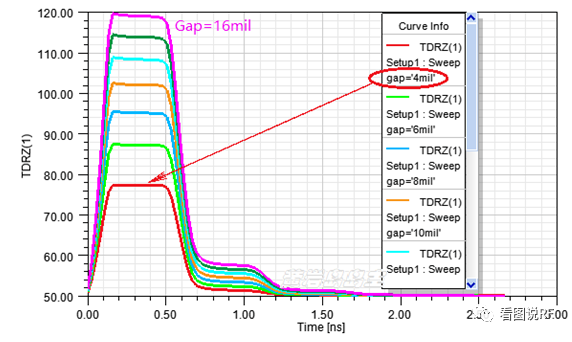
2.4 Signal Reflection in High-Speed Designs
In RF and high-speed PCBs, improper copper pour can cause impedance mismatches. Solution:
- Simulate impedance effects before finalizing the design.
- Avoid large copper gaps under critical transmission lines.
3. Best Practices for Effective Copper Pour Implementation
To maximize the benefits while minimizing risks, designers should follow these guidelines:
3.1 Proper Grounding Strategy
- Use a Solid Ground Plane: Ensure low-impedance return paths for signals.
- Avoid Floating Copper: Always connect copper pour to a net (usually ground) to prevent antenna effects.
3.2 Thermal Relief for Component Pads
- Prevent Cold Solder Joints: Use thermal spokes for component pads to ensure proper soldering.
3.3 Optimizing Copper Pour Clearance
- Maintain Adequate Spacing: Follow IPC standards for clearance between copper and traces.
- Use Anti-Pads for Vias: Prevent unintended connections in high-density designs.
3.4 Simulation and Verification
- Perform Signal Integrity Analysis: Use tools like HyperLynx or Ansys SIwave to assess copper pour impact.
- Check for Manufacturing Feasibility: Validate designs with PCB fabricators.
4. Conclusion
Copper pour is an essential technique in PCB design, offering significant advantages in signal integrity, thermal management, EMC, and manufacturability. However, improper application can introduce challenges such as parasitic effects and manufacturing defects. By following best practices—such as proper grounding, thermal relief, and simulation—designers can leverage copper pour effectively to enhance PCB performance and reliability.
As PCB technology evolves with higher speeds and miniaturization, the strategic use of copper pour will remain a critical factor in achieving optimal electronic designs.