The PCB Drilling Process: A Comprehensive Guide
Introduction to PCB Drilling
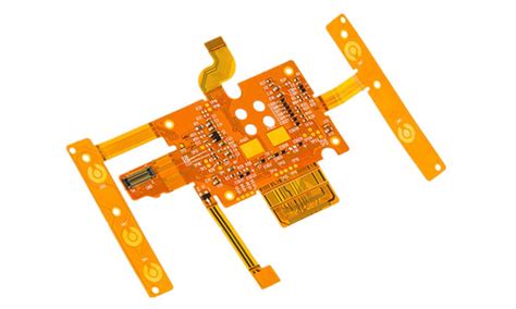
Printed Circuit Board (PCB) drilling is a critical manufacturing process that creates holes in PCBs to establish electrical connections between different layers or to mount components. As modern electronics continue to become more complex and miniaturized, the importance of precise, reliable drilling processes has grown exponentially. The PCB drilling process accounts for approximately 30-40% of the total board manufacturing cost, making it one of the most significant steps in PCB production.
This article provides a detailed examination of the PCB drilling process, covering drill bit types, drilling methods, quality control measures, and emerging technologies in the field. Understanding these aspects is essential for PCB designers, manufacturing engineers, and quality assurance professionals working in the electronics industry.
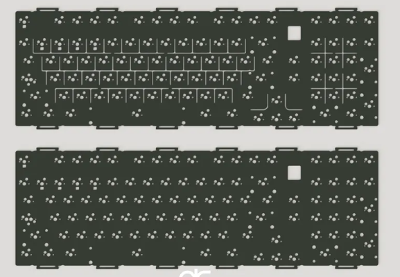
Types of Holes in PCBs
Before delving into the drilling process itself, it’s important to understand the different types of holes found in PCBs:
1. Through Holes
These holes penetrate all layers of the PCB and are typically used for two purposes:
- Component leads: For mounting through-hole components
- Vias: For creating electrical connections between layers
2. Blind Vias
These holes connect an outer layer to one or more inner layers but do not go through the entire board.
3. Buried Vias
These vias connect inner layers without reaching either surface of the PCB.
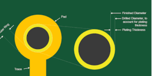
4. Microvias
With diameters typically less than 150 microns (6 mils), these small holes are used in high-density interconnect (HDI) PCBs.
The type of hole required significantly influences the choice of drilling method and equipment.
PCB Drill Bit Types and Characteristics
The selection of appropriate drill bits is crucial for achieving high-quality holes. PCB drill bits differ from conventional drill bits in several ways:
1. Materials
- Solid Carbide: The most common material for PCB drilling due to its hardness and wear resistance
- Diamond-coated: Used for abrasive materials like ceramic-filled laminates
- Special alloys: For particularly challenging materials
2. Geometry
PCB drill bits feature:
- Special flute designs for efficient chip removal
- Precise point angles (typically 130°-140°)
- Ultra-fine tolerances (often within ±5 microns)
3. Sizes
PCB drills range from:
- Standard sizes (0.2mm to 6.5mm)
- Microdrills (below 0.2mm) for HDI applications
4. Coatings
Various coatings enhance performance:
- Titanium Nitride (TiN) for increased hardness
- Titanium Aluminum Nitride (TiAlN) for higher temperature resistance
- Diamond-like carbon (DLC) for reduced friction
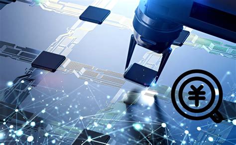
The PCB Drilling Process: Step-by-Step
1. Preparation Phase
- Data Preparation: Conversion of design files to machine-readable drill files (typically Excellon format)
- Panelization: Arrangement of multiple PCBs on a panel for efficient drilling
- Tool Selection: Choosing appropriate drill bits based on hole sizes and materials
- Machine Setup: Loading drill bits, setting parameters (speed, feed rate, etc.)
2. Drilling Operation
The actual drilling process involves several critical steps:
A. Entry Material Application
A sacrificial material (typically aluminum foil or composite entry material) is placed on top of the PCB stack to:
- Prevent drill bit wandering during entry
- Reduce burr formation
- Protect the board surface
B. Drilling Parameters
Optimal parameters vary by material and drill size but generally include:
- Spindle Speed: 80,000-150,000 RPM for small drills
- Feed Rate: 1-5 μm/revolution
- Retract Rate: Faster than feed rate to minimize heat buildup
- Peck Drilling: For deep holes or difficult materials
C. Hole Formation
The drilling mechanism:
- The rotating drill bit penetrates the entry material
- Progresses through the PCB laminate
- Exits through the backup material (typically phenolic)
D. Chip Removal
Effective chip evacuation is critical:
- Compressed air blows chips away from the hole
- Vacuum systems remove debris from the work area
- Regular bit cleaning prevents chip packing
3. Post-Drilling Processes
After drilling, several important steps follow:
- Deburring: Removal of rough edges around holes
- Desmearing: Elimination of resin smear from hole walls
- Cleaning: Removal of drilling debris
- Inspection: Verification of hole quality and position accuracy
PCB Drilling Methods
Several drilling technologies are employed in PCB manufacturing:
1. Mechanical Drilling
The most common method, using rotating carbide bits:
- Advantages: High precision, good surface finish, cost-effective for standard holes
- Limitations: Wear issues with small drills (<0.2mm), limited aspect ratios
2. Laser Drilling
Used primarily for microvias and HDI applications:
- Types: CO₂ lasers (for organic materials), UV lasers (for smaller, more precise holes)
- Advantages: No physical drill wear, extremely small holes possible
- Limitations: Higher equipment cost, slower for larger holes
3. Plasma Etching
A non-contact method for creating small vias:
- Advantages: No mechanical stress, simultaneous processing of multiple holes
- Limitations: Limited to certain materials, tapered hole profiles
4. Photoimaging
A chemical process for creating very small vias:
- Advantages: Extremely small features possible, no physical drilling
- Limitations: Complex process, limited to specific applications
Quality Control in PCB Drilling
Maintaining high quality in drilled holes is essential for PCB reliability. Key quality parameters include:
1. Dimensional Accuracy
- Hole diameter (typically ±50μm tolerance)
- Hole position accuracy (often ±25μm)
- Roundness (deviation from perfect circularity)
2. Hole Wall Quality
- Surface roughness
- Presence of resin smear
- Glass fiber protrusions
3. Metallization Readiness
- Cleanliness of hole walls for subsequent plating
- Absence of debris or contamination
Quality control methods include:
- Automated Optical Inspection (AOI): For hole position and size verification
- Cross-sectioning: For evaluating hole wall quality
- Electrical testing: For continuity of plated through holes
Common Drilling Defects and Solutions
Several defects can occur during PCB drilling:
1. Drill Breakage
- Causes: Excessive feed rate, worn drills, improper chip evacuation
- Solutions: Optimize parameters, implement drill wear monitoring
2. Hole Wall Roughness
- Causes: Dull drills, improper feed/speed, material issues
- Solutions: Use sharper drills, adjust parameters, consider alternative materials
3. Resin Smear
- Causes: Excessive heat during drilling
- Solutions: Optimize drilling parameters, use appropriate entry/backup materials
4. Nailheading
- Causes: Excessive drill wear, improper backup
- Solutions: Regular drill replacement, improved backup materials
5. Barrel Cracking
- Causes: Mechanical stress during drilling
- Solutions: Adjust feed rates, consider alternative drilling methods
Advanced Drilling Technologies
Recent advancements in PCB drilling include:
1. High-Speed Spindles
- Air-bearing spindles reaching 300,000 RPM
- Improved precision for microdrilling applications
2. Automated Drill Change Systems
- Reduce setup times
- Enable more frequent drill changes for consistent quality
3. In-Process Monitoring
- Vibration sensors for detecting drill wear
- Acoustic emission monitoring for breakage detection
4. Laser Direct Drilling
- Eliminates photolithography steps for via formation
- Enables finer pitch interconnects
5. Adaptive Control Systems
- Real-time adjustment of drilling parameters
- Compensation for material variations
Environmental and Safety Considerations
PCB drilling presents several environmental and safety challenges:
1. Dust Collection
- Drilling generates fine dust particles (including glass fibers)
- High-efficiency particulate air (HEPA) filtration systems are essential
2. Noise Control
- High-speed spindles produce significant noise
- Enclosures and hearing protection are necessary
3. Coolant Systems
- Some applications require coolant for heat management
- Proper handling and disposal of coolants is critical
4. Energy Efficiency
- Modern drilling machines incorporate energy-saving features
- Smart scheduling reduces idle time
Future Trends in PCB Drilling
The PCB drilling landscape continues to evolve:
1. Increased Automation
- Fully automated drilling lines with minimal human intervention
- Integration with other PCB manufacturing processes
2. Smaller Feature Sizes
- Continued reduction in via sizes (below 50μm)
- Development of new drilling technologies for nanometer-scale features
3. Alternative Materials
- Drilling solutions for new substrate materials (flexible, ceramic, etc.)
- Adaptive processes for heterogeneous material stacks
4. Industry 4.0 Integration
- IoT-enabled drilling machines
- Predictive maintenance based on real-time data analytics
5. Sustainable Practices
- Reduced material waste
- Energy-efficient drilling processes
- Recyclable drill bits and consumables
Conclusion
The PCB drilling process is a complex, precision operation that plays a vital role in the manufacture of reliable electronic circuits. As PCBs continue to increase in complexity and density, drilling technologies must advance to meet these challenges. Understanding the fundamentals of PCB drilling—from drill bit selection to quality control—enables manufacturers to produce higher quality boards with greater efficiency.
The future of PCB drilling lies in the integration of advanced technologies, increased automation, and sustainable practices. By staying abreast of these developments, PCB manufacturers can maintain competitiveness in an ever-evolving electronics industry. Whether through mechanical means or alternative drilling technologies, the creation of precise, reliable holes remains fundamental to PCB manufacturing and will continue to be an area of significant innovation.