The PCB Prototyping Process: A Comprehensive Guide
Introduction to PCB Prototyping
Printed Circuit Board (PCB) prototyping is an essential phase in electronics development that bridges the conceptual design and mass production stages. This critical process allows engineers and designers to verify their circuit designs, test functionality, and identify potential issues before committing to large-scale manufacturing. PCB prototyping has evolved significantly with advancements in technology, enabling faster turnaround times and higher precision than ever before.
The prototyping phase serves multiple purposes in product development. It provides tangible proof of concept, allows for performance testing under real-world conditions, and enables design optimization. For startups and established companies alike, effective PCB prototyping can mean the difference between a successful product launch and costly redesigns.
Modern PCB prototyping services offer various options to suit different project requirements, ranging from simple single-layer boards to complex multi-layer designs with advanced features like blind vias and impedance control. Understanding the complete prototyping workflow helps designers make informed decisions at each stage of development.
Design Preparation and File Submission
The PCB prototyping process begins with careful design preparation using Electronic Design Automation (EDA) software. Popular tools include Altium Designer, KiCad, Eagle, and OrCAD. These applications allow designers to create schematic diagrams, convert them to board layouts, and generate all necessary files for manufacturing.
When the design is complete, several critical files must be prepared for submission to the prototyping service:
- Gerber Files: The industry-standard RS-274X format contains all layer information including copper traces, solder mask, and silkscreen. Each layer (top copper, bottom copper, inner layers, etc.) requires a separate Gerber file.
- Drill Files: Excellon format files specify hole sizes and locations for through-holes and vias.
- Board Outline File: Defines the physical shape and dimensions of the PCB.
- Pick-and-Place File: For assembled boards, this file provides component locations and orientations.
- Bill of Materials (BOM): Lists all components with their specifications and reference designators.
Many prototyping services now accept native design files (like .brd or .PcbDoc) and handle the Gerber conversion internally, reducing potential errors in file generation. However, it remains crucial to verify all files before submission using Gerber viewers or the manufacturer’s online inspection tools.
Material Selection and Stackup Configuration
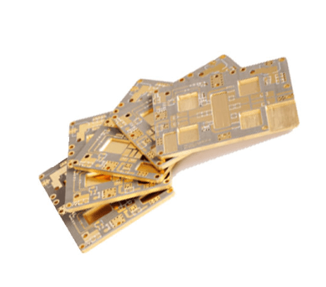
Choosing appropriate materials is fundamental to PCB performance and reliability. Standard FR-4 (Flame Retardant 4) epoxy laminate serves as the most common base material for prototypes, offering good mechanical and electrical properties at reasonable cost. For high-frequency applications, specialized materials like Rogers or Teflon may be necessary to maintain signal integrity.
The stackup configuration determines how copper layers and insulating material are arranged in multilayer boards. Key considerations include:
- Layer Count: Ranging from single-sided to complex 16+ layer boards
- Copper Weight: Typically 0.5 oz to 2 oz per square foot (17 μm to 70 μm)
- Dielectric Thickness: Between layers, affecting impedance and crosstalk
- Surface Finish: Options include HASL (Hot Air Solder Leveling), ENIG (Electroless Nickel Immersion Gold), and OSP (Organic Solderability Preservative)
For prototypes intended to closely match final production boards, it’s advisable to use the same materials and stackup as planned for mass production. Many manufacturers offer online stackup calculators to help designers achieve target impedances and meet other electrical requirements.
Manufacturing Process Overview
Once design files are submitted and materials selected, the PCB prototype undergoes several manufacturing stages:
1. Imaging and Etching
The process begins with transferring the circuit pattern onto copper-clad laminate. Photolithography techniques expose photoresist to UV light through a photomask (created from Gerber files), then develop the image. Chemical etching removes unwanted copper, leaving only the desired traces.
2. Layer Alignment and Lamination
For multilayer boards, individual layers must be precisely aligned using registration holes before lamination. High pressure and temperature bond the layers together with prepreg (pre-impregnated) dielectric material.
3. Drilling
Mechanical or laser drills create holes for through-hole components and vias based on the submitted drill files. Advanced HDI (High Density Interconnect) boards may require laser drilling for microvias.
4. Plating and Surface Finish
Holes are plated with copper to establish electrical connections between layers. The board then receives its chosen surface finish to protect copper and ensure solderability.
5. Solder Mask Application
A liquid photoimageable solder mask is applied and cured, exposing only areas where components will be soldered. This layer prevents solder bridges and protects copper from oxidation.
6. Silkscreen Printing
Component designators, logos, and other markings are printed on the board surface using epoxy ink. This aids assembly and debugging.
7. Electrical Testing
Basic continuity testing verifies no open or short circuits exist. More advanced prototypes may undergo flying probe or fixture testing to check impedance and functionality.
8. Routing and Scoring
Individual boards are separated from the production panel using routing bits or scoring tools, creating the final board outline.
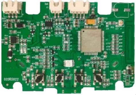
Assembly Options for Prototypes
Many PCB prototyping services offer assembly options to deliver fully functional boards:
1. Turnkey Assembly
The service provider sources all components and completes the entire assembly process. This is the most convenient but least flexible option.
2. Partial Assembly
Customers may supply some or all components, particularly for hard-to-find or proprietary parts. This approach offers cost savings when certain components are already available.
3. Kitted Assembly
Customers provide all components pre-sorted and labeled for each board. The manufacturer handles only the placement and soldering.
Assembly processes include:
- Solder Paste Application: Stencil printing or jetting deposits precise amounts of solder paste on pads
- Component Placement: Pick-and-place machines position SMD components at high speed
- Reflow Soldering: The board passes through a reflow oven to melt solder and create permanent connections
- Through-Hole Component Insertion: For mixed-technology boards, wave soldering or hand soldering completes the assembly
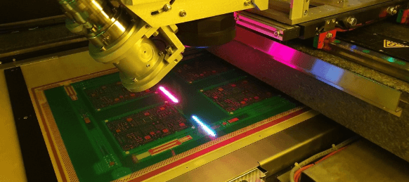
- Inspection: Automated optical inspection (AOI) and X-ray verify proper component placement and solder joints
Quality Control and Testing Procedures
Reliable prototyping services implement multiple quality control measures throughout production:
- Automated Optical Inspection (AOI): Cameras compare manufactured boards to design files, identifying defects like missing traces or incorrect drill sizes.
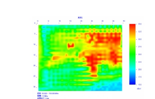
- Electrical Testing: Continuity tests check for opens and shorts, while more advanced testing may verify impedance and high-speed signal integrity.
- Microsection Analysis: Cross-sectioning sample boards examines internal layer alignment and plating quality.
- Solderability Testing: Ensures proper surface finish application for reliable component attachment.
- Environmental Stress Testing: Some prototypes undergo thermal cycling or humidity exposure to verify reliability.
For assembled boards, additional testing includes:
- In-Circuit Testing (ICT) verifying component values and orientations
- Functional testing under real operating conditions
- Boundary scan testing for complex digital circuits
Turnaround Time Considerations
PCB prototyping services offer various turnaround options to meet different project needs:
- Standard Lead Time: Typically 5-7 business days, offering the best balance of cost and speed.
- Express Service: 2-3 day turnaround for projects needing faster iteration, at a premium price.
- Same-Day Service: Available from some providers for extremely urgent prototypes with simple designs.
- Weekend Service: Some manufacturers operate weekend shifts to deliver Monday morning.
Factors affecting turnaround time include:
- Board complexity (layer count, special features)
- Material availability
- Current shop workload
- Shipping method selected
When planning development schedules, it’s wise to account for potential re-spins. Even well-designed boards may require 2-3 iterations to resolve all issues.
Cost Factors in PCB Prototyping
Prototyping costs vary significantly based on multiple factors:
- Board Size: Larger boards use more material and reduce panel utilization.
- Layer Count: Each additional layer increases processing steps and material costs.
- Quantity: Unit cost decreases with higher quantities due to fixed setup costs.
- Material Choice: Standard FR-4 is most economical; high-frequency or flexible materials cost more.
- Special Features: Impedance control, blind/buried vias, and thick copper add expense.
- Surface Finish: ENIG costs more than HASL but provides better results for fine-pitch components.
- Solder Mask Color: Standard green is cheapest; other colors may incur additional charges.
- Testing Requirements: More comprehensive testing increases cost but improves reliability.
Many manufacturers offer online instant quoting tools that calculate pricing based on uploaded design files and selected options. For budget-conscious projects, designers can often reduce costs by:
- Minimizing board size
- Using standard materials and finishes
- Avoiding unnecessary special requirements
- Ordering multiple prototypes at once when possible
Common Prototyping Challenges and Solutions
Even experienced engineers encounter challenges during PCB prototyping:
1. Design Rule Violations
Solution: Carefully review manufacturer’s capabilities and design rules before submission. Use DRC (Design Rule Check) tools in EDA software.
2. Impedance Mismatches
Solution: Provide complete stackup information and use manufacturer’s impedance calculators. Request impedance testing for critical traces.
3. Assembly Difficulties
Solution: Follow component spacing guidelines, provide accurate footprints, and consider assembly requirements during layout.
4. Signal Integrity Issues
Solution: Prototype early with proper high-speed design techniques. Use reference planes and controlled impedance where needed.
5. Thermal Management Problems
Solution: Incorporate thermal relief in designs, use adequate copper pours, and consider thermal vias for heat dissipation.
6. Manufacturing Defects
Solution: Work with reputable suppliers, provide clear documentation, and request design for manufacturability (DFM) feedback.
Future Trends in PCB Prototyping
The PCB prototyping industry continues to evolve with several emerging trends:
- Additive Manufacturing: Inkjet and aerosol jet printing enable faster turnaround for simple boards without traditional etching.
- Embedded Components: Passive components integrated within the PCB substrate reduce surface area needs.
- Advanced Materials: New dielectric materials support higher frequencies and better thermal performance.
- AI-Assisted Design: Machine learning algorithms help optimize layouts and predict potential issues.
- Cloud-Based Collaboration: Design teams work simultaneously on shared projects with real-time updates.
- Enhanced Testing Automation: More sophisticated test fixtures and algorithms improve quality control.
- Sustainable Practices: Eco-friendly materials and processes reduce environmental impact.
These advancements promise to make PCB prototyping even faster, more reliable, and accessible to a broader range of innovators.
Conclusion
PCB prototyping serves as the critical bridge between electronic design concepts and final products. By understanding the complete prototyping workflow—from design preparation through manufacturing and testing—engineers can make informed decisions that optimize both performance and cost-effectiveness. Modern prototyping services offer unprecedented capabilities, allowing designers to quickly iterate and refine their products before committing to full-scale production.
As technology advances, PCB prototyping continues to become more sophisticated, with shorter lead times, higher quality, and greater flexibility. Whether developing simple consumer devices or complex aerospace systems, a solid grasp of prototyping principles remains essential for successful electronic product development. By leveraging available tools and services while adhering to design best practices, engineering teams can significantly reduce development risks and bring better products to market faster.