The Relationship Between Copper Foil and Current Flow in PCB Design
Abstract
This paper explores the critical relationship between copper foil properties and current flow characteristics in printed circuit board (PCB) design. As electronic devices continue to shrink in size while increasing in performance, understanding this relationship becomes paramount for designing reliable, efficient PCBs. The discussion covers copper foil types, thickness selection, current carrying capacity, thermal considerations, and high-frequency effects. Practical design guidelines are provided to help engineers optimize their PCB layouts for various applications.

1. Introduction
Printed Circuit Boards (PCBs) serve as the foundation of modern electronics, providing both mechanical support and electrical connections between components. At the heart of every PCB’s functionality lies the copper foil that forms its conductive pathways. The relationship between copper foil properties and current flow characteristics directly impacts a PCB’s performance, reliability, and longevity.
As electronic devices become more compact and powerful, PCB designers face increasing challenges in managing current flow through copper traces. Insufficient copper can lead to excessive heating and voltage drops, while excessive copper wastes space and increases cost. This paper examines the fundamental principles governing this relationship and provides practical design considerations.
2. Copper Foil Fundamentals
2.1 Types of Copper Foil
PCB manufacturers typically use two main types of copper foil:
- Electrodeposited (ED) Copper: Created through an electrochemical process, ED copper has a columnar grain structure with rough surfaces that enhance adhesion to the substrate. The roughness, however, can affect high-frequency performance.
- Rolled Annealed (RA) Copper: Produced by physically rolling copper ingots, RA copper has a smoother surface and more uniform grain structure, making it preferable for high-frequency applications.
2.2 Copper Weight and Thickness
Copper foil thickness is commonly specified in ounces per square foot (oz/ft²), representing the weight of copper covering one square foot of area:
- 1 oz/ft² ≈ 35 μm thickness
- 2 oz/ft² ≈ 70 μm thickness
- 0.5 oz/ft² ≈ 17.5 μm thickness
The choice of copper weight affects current carrying capacity, thermal performance, and manufacturability.
3. Current Flow Characteristics
3.1 DC Current Considerations
For DC current applications, the primary concerns are:
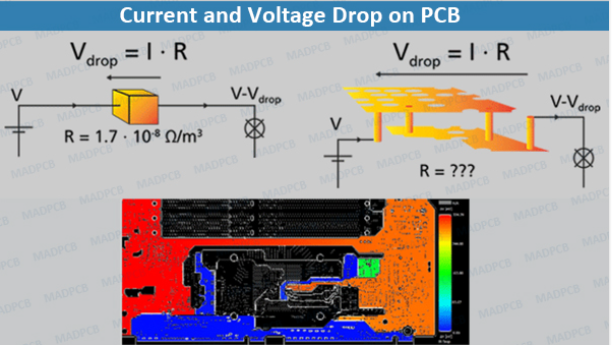
- Current Carrying Capacity: The maximum current a trace can handle without excessive temperature rise.
- Voltage Drop: The potential difference along a trace due to its resistance.
- Power Dissipation: The heat generated by current flowing through trace resistance.
The resistance of a copper trace is given by:
R = ρ × (L / A)
Where:
- R = resistance (Ω)
- ρ = resistivity of copper (1.72×10⁻⁶ Ω-cm at 20°C)
- L = trace length (cm)
- A = cross-sectional area (cm²)
3.2 AC and High-Frequency Considerations
At higher frequencies, additional phenomena affect current flow:
- Skin Effect: Current tends to flow near the surface of conductors at high frequencies, effectively reducing the usable cross-section.
- Proximity Effect: Nearby conductors influence current distribution, potentially increasing AC resistance.
- Return Path Considerations: High-frequency currents follow the path of least impedance, which often means the closest return path rather than the shortest geometric path.
The skin depth (δ) can be calculated as:
δ = √(ρ / (π × μ × f))
Where:
- ρ = resistivity (Ω-m)
- μ = permeability (H/m)
- f = frequency (Hz)
For copper at room temperature, this simplifies to approximately:
δ ≈ 6.6 / √f cm (with f in Hz)
4. Thermal Considerations
4.1 Temperature Rise
Current flowing through copper traces generates heat due to resistive losses. The temperature rise depends on:
- Current magnitude
- Trace resistance
- Thermal dissipation properties
- Ambient temperature
IPC-2152 provides standards for determining current limits based on allowable temperature rise.
4.2 Thermal Management Techniques
To manage heat in high-current designs:
- Increase Copper Weight: Thicker copper reduces resistance and improves heat dissipation.
- Use Thermal Reliefs: For component pads connected to large copper areas.
- Incorporate Heat Sinks: Additional copper pours or metal structures to dissipate heat.
- Optimize Board Stackup: Strategic placement of power and ground planes for heat spreading.
5. Design Guidelines
5.1 Trace Width Calculations
Several methods exist for determining appropriate trace widths:
- IPC-2152 Nomographs: Graphical tools for determining current capacity based on copper weight, temperature rise, and trace width.
- Empirical Formulas: Such as the modified version of the IPC-2221 formula:
I = k × ΔT⁰·⁴⁴ × A⁰·⁷²⁵
Where:
- I = current (A)
- ΔT = temperature rise (°C)
- A = cross-sectional area (mil²)
- k = 0.048 for outer layers, 0.024 for inner layers
5.2 High-Current Design Techniques
For high-current applications:
- Use Multiple Layers: Distribute current across several layers connected with multiple vias.
- Employ Copper Pours: Large areas of copper reduce resistance and improve heat dissipation.
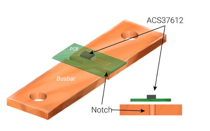
- Consider Bus Bars: For extremely high currents, supplemental bus bars may be necessary.
- Minimize Sharp Corners: To avoid current crowding effects.
5.3 High-Frequency Design Techniques
For high-frequency applications:
- Use Smooth Copper: Rolled annealed copper minimizes surface roughness losses.
- Control Impedance: Carefully calculate trace dimensions for proper characteristic impedance.
- Optimize Return Paths: Ensure continuous reference planes beneath signal traces.
- Minimize Discontinuities: Avoid sharp bends and impedance mismatches.
6. Advanced Considerations
6.1 Current Crowding
Current tends to concentrate in certain areas:
- Trace Corners: Current density increases at inner radii of bends.
- Via Transitions: Current crowds at the entrance and exit points of vias.
- Junctions: T-junctions and other trace intersections create non-uniform current distribution.
6.2 Electromigration
At high current densities (typically > 10⁵ A/cm²), copper atoms can migrate, leading to:
- Void Formation: Thinning of conductors in some areas.
- Dendrite Growth: Copper accumulation in other areas.
- Eventual Open Circuits: Complete failure of the conductor.
6.3 Manufacturing Tolerances
Actual copper thickness can vary due to:
- Etching Process: Over-etching can reduce final copper thickness.
- Plating Variations: Electroplated finishes may not be perfectly uniform.
- Surface Treatments: Final finishes (ENIG, HASL, etc.) affect effective conductivity.
Designers should account for these tolerances in critical applications.

7. Case Studies
7.1 Power Distribution Network
A 4-layer PCB for a 50A power supply demonstrates:
- Inner Layer Current Distribution: Using 2 oz copper on inner layers for bulk current carrying.
- Via Arrays: Multiple large vias to transfer current between layers.
- Thermal Relief: Strategic copper pours connected to component pads.
7.2 High-Speed Digital Design
A 10 Gbps serial link illustrates:
- Controlled Impedance: Precise trace width and spacing for 100Ω differential pairs.
- Return Path Optimization: Uninterrupted ground plane beneath signal traces.
- Skin Effect Mitigation: Use of wider traces than DC calculations would suggest.
8. Conclusion
The relationship between copper foil and current flow in PCB design is complex and multifaceted. Designers must consider electrical, thermal, and manufacturing factors when selecting copper weights and determining trace geometries. As technology advances, with currents increasing and device sizes decreasing, this relationship becomes even more critical to understand and optimize.
Future trends may include:
- Thicker Copper Substrates: For high-power applications.
- Embedded Bus Structures: For better current distribution.
- Advanced Materials: Copper alloys with better high-frequency performance.
- 3D Current Flow Analysis: More sophisticated simulation tools.
By thoroughly understanding the principles discussed in this paper, PCB designers can create more reliable, efficient boards that meet the demanding requirements of modern electronics.