The Relationship Between PCB Copper Area and Thermal Resistance: A Comprehensive Analysis
Abstract
This paper explores the critical relationship between copper surface area on printed circuit boards (PCBs) and thermal resistance, examining how proper copper allocation and design can significantly improve thermal management in electronic devices. Through theoretical analysis and practical considerations, we demonstrate how engineers can optimize PCB layouts to enhance heat dissipation while maintaining electrical performance and cost efficiency.
1. Introduction
In modern electronics design, thermal management has become as crucial as electrical performance, particularly with increasing component density and power requirements. The copper layers in PCBs serve dual purposes: providing electrical connectivity and acting as heat dissipation pathways. Understanding the relationship between copper area and thermal resistance is fundamental for designing reliable electronic systems.
Thermal resistance (θ) represents a material’s opposition to heat flow, measured in °C/W. In PCBs, lower thermal resistance between heat-generating components and the environment means more efficient heat dissipation. Copper, with its excellent thermal conductivity (385 W/mK at 20°C), plays a pivotal role in this thermal pathway.
2. Fundamentals of PCB Thermal Transfer
2.1 Heat Transfer Mechanisms in PCBs
Three primary mechanisms govern heat transfer in PCBs:
- Conduction: Dominant mechanism through copper traces and planes
- Convection: Heat transfer to surrounding air from PCB surfaces
- Radiation: Typically minor contributor except in high-temperature or vacuum applications
Copper areas affect all three mechanisms but particularly influence conduction and convection by providing both thermal pathways and surface area for air interaction.
2.2 Thermal Resistance Network
The total thermal resistance (θ_JA) from junction to ambient consists of:
- θ_JC (junction to case)
- θ_CS (case to heatsink/surface)
- θ_SA (heatsink/surface to ambient)
Copper areas primarily affect θ_CS and θ_SA by providing lower-resistance paths and greater surface area for convection.
3. Copper Area and Thermal Resistance Relationship
3.1 Theoretical Basis
The thermal resistance of a copper plane can be modeled as:
θ = L / (k × A)
Where:
- θ = thermal resistance (°C/W)
- L = length of thermal path (m)
- k = thermal conductivity of copper (385 W/mK)
- A = cross-sectional area (m²)
For a given thickness, increasing copper area directly reduces thermal resistance by increasing A in this equation.
3.2 Practical Considerations
In actual PCB applications, the relationship is more complex due to:
- Non-uniform heat distribution: Heat sources aren’t perfectly distributed across the copper area
- Boundary conditions: Edge effects and connection points modify ideal behavior
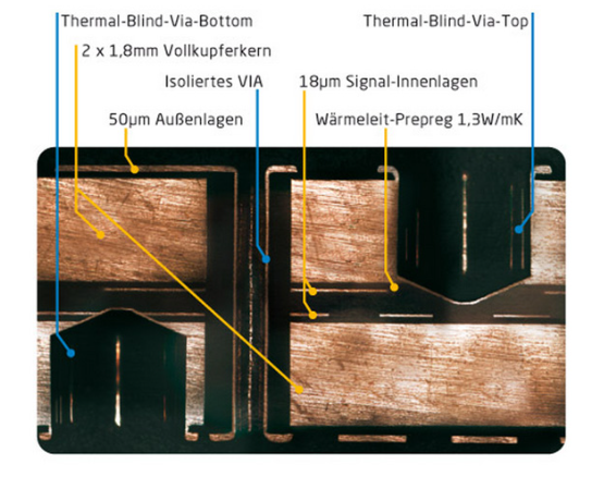
- Layer stacking: Multi-layer boards create complex 3D thermal paths
- Via influence: Thermal vias between layers affect overall resistance
3.3 Empirical Observations
Studies have shown that for typical FR-4 PCBs:
- Doubling copper area can reduce θ_JA by 30-40%
- The benefit diminishes as area increases (logarithmic relationship)
- 1 oz (35 μm) copper shows about 15% higher θ than 2 oz copper for same area
4. Calculating Required Copper Area
4.1 Basic Calculation Method
A simplified approach to estimate required copper area for a given thermal resistance:
A = (P × θ_desired × k) / ΔT
Where:
- P = power dissipation (W)
- θ_desired = target thermal resistance (°C/W)
- ΔT = allowable temperature rise (°C)
4.2 Advanced Modeling Techniques
For more accurate results, engineers use:
- Finite Element Analysis (FEA): Detailed numerical modeling
- Computational Fluid Dynamics (CFD): Accounts for air flow and convection
- Industry-standard tools: Ansys Icepak, FloTHERM, etc.
4.3 Design Rules of Thumb
Practical guidelines suggest:
- Minimum 1 in² (6.45 cm²) of copper per watt for moderate cooling
- 2-3 in² per watt for better performance
- Additional area needed for high-power components
5. Copper Allocation Strategies
5.1 Copper Thickness Selection
Common options and their impact:
| Copper Weight | Thickness | Thermal Performance |
|---|---|---|
| 0.5 oz | 17.5 μm | Basic, low cost |
| 1 oz | 35 μm | Standard balance |
| 2 oz | 70 μm | Improved thermal |
| 3 oz+ | 105 μm+ | High power apps |
5.2 Copper Distribution Techniques
Effective strategies include:
- Thermal relief patterns: Balancing electrical and thermal needs
- Filled vias: Enhancing vertical heat transfer
- Copper balancing: Maintaining even distribution for manufacturability
- Zone allocation: Concentrating copper near heat sources
5.3 Multi-layer Considerations
In complex PCBs:
- Inner layers contribute about 30-50% of surface layer effectiveness
- Proper via placement is crucial for utilizing all layers
- Power and ground planes serve as excellent thermal pathways

6. Special Cases and Advanced Techniques
6.1 High-Power Applications
For power electronics (>10W components):
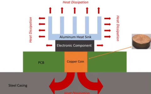
- Dedicated thermal pads (exposed copper)
- Metal core PCBs or insulated metal substrates
- Direct bonding to heatsinks
6.2 High-Density Designs
When space is limited:
- Microvias for enhanced vertical conduction
- Thermal interface materials
- Selective thick copper plating
6.3 RF and High-Frequency Considerations
Balancing thermal needs with:
- Skin effect requirements
- Impedance control
- Signal integrity constraints
7. Measurement and Verification
7.1 Laboratory Techniques
Common measurement approaches:
- Infrared thermography: Visualizing temperature distribution
- Thermal couples: Point measurements
- Thermal test dies: Standardized components for testing
7.2 Correlation with Models
Important to validate simulations with:
- Prototype testing
- Boundary condition verification
- Environmental factor consideration
8. Cost-Benefit Analysis
8.1 Manufacturing Trade-offs
Factors affecting decisions:
- Additional copper increases cost (material and processing)
- Thicker copper requires adjusted etching processes
- Balance between copper area and board size
8.2 Reliability Implications
Proper thermal design affects:
- Mean time between failures (MTBF)
- Thermal cycling endurance
- Long-term performance stability
9. Future Trends
Emerging developments impacting this relationship:
- Embedded cooling technologies: Microchannels, two-phase cooling
- Advanced materials: Graphene-enhanced substrates
- Additive manufacturing: Novel copper deposition techniques
- 3D packaging: Vertical integration challenges
10. Conclusion
The relationship between PCB copper area and thermal resistance is fundamental to modern electronics design. Through careful analysis and optimization of copper allocation, engineers can significantly improve thermal performance without necessarily increasing costs or board size. As power densities continue to rise, innovative approaches to utilizing copper for thermal management will remain essential for reliable electronic systems.
Future work should focus on developing more accurate predictive models that account for complex multi-physics interactions while providing practical design guidelines for increasingly challenging thermal environments.