The Relationship Between Power Supply Layout and EMC
Abstract
Electromagnetic Compatibility (EMC) is a critical consideration in modern electronic design, ensuring that devices operate without interfering with other systems or being affected by external electromagnetic disturbances. One of the key factors influencing EMC performance is the layout of the power supply circuitry. This paper explores the relationship between power supply layout and EMC, discussing key design principles, common issues, and mitigation techniques to achieve optimal EMC performance.
1. Introduction
With the increasing complexity and miniaturization of electronic systems, managing electromagnetic interference (EMI) has become a significant challenge. The power supply, being a primary source of both conducted and radiated emissions, plays a crucial role in determining a system’s EMC performance. Poor power supply layout can lead to excessive noise, ground loops, and unintended coupling paths, degrading signal integrity and causing compliance failures in regulatory standards such as CISPR, FCC, and IEC.
This paper examines how power supply layout affects EMC, focusing on key aspects such as grounding strategies, component placement, trace routing, and decoupling techniques.
2. Fundamentals of EMC in Power Supply Design
EMC encompasses two main aspects:
- Emissions (EMI): Unintended electromagnetic noise generated by the system.
- Susceptibility (Immunity): The system’s ability to resist external electromagnetic disturbances.
The power supply contributes to both aspects due to:
- High-frequency switching (in switch-mode power supplies, SMPS).
- Large current loops that can act as antennas.
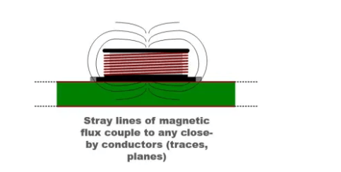
- Parasitic inductances and capacitances in PCB traces.
A well-optimized power supply layout minimizes these effects by controlling current return paths, reducing loop areas, and suppressing high-frequency noise.
3. Key Power Supply Layout Considerations for EMC
3.1 Grounding Strategies
Proper grounding is essential for minimizing EMI. Common techniques include:
- Single-Point Grounding: Effective for low-frequency circuits to avoid ground loops.
- Multi-Point Grounding: Used in high-frequency designs to reduce impedance.
- Ground Plane Usage: A solid ground plane provides a low-impedance return path and reduces loop area.
Improper grounding can lead to ground bounce and common-mode noise, worsening EMC performance.
3.2 Component Placement
- Decoupling Capacitors: Placed as close as possible to IC power pins to minimize high-frequency noise.
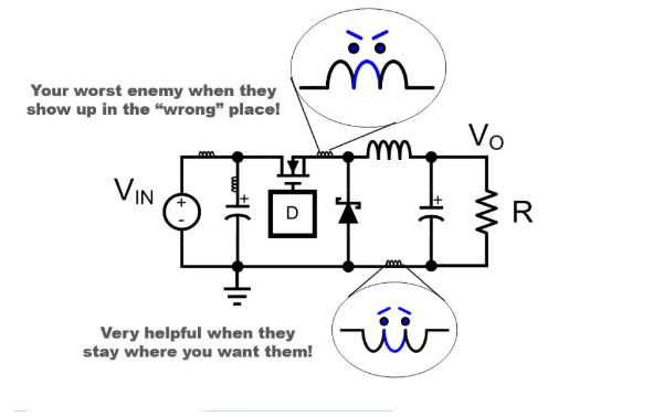
- Switching Components (MOSFETs, Diodes): Positioned to minimize parasitic inductance in high-current paths.
- Filter Components (Ferrite Beads, Inductors): Used to block high-frequency noise from propagating.
3.3 Trace Routing Techniques
- Minimizing Loop Area: High-current loops should be kept small to reduce radiated emissions.
- Avoiding Parallel High-Speed Traces: Crosstalk can be minimized by separating noisy and sensitive traces.
- Using Wide Traces for High Current: Reduces parasitic resistance and inductance.
3.4 Shielding and Filtering
- Shielding: Metal enclosures or PCB shields can contain radiated emissions.
- Input/Output Filtering: LC filters and common-mode chokes suppress conducted EMI.
4. Common EMC Issues Due to Poor Power Supply Layout
4.1 Radiated Emissions from High-Frequency Switching
Switching power supplies generate high-frequency harmonics that can radiate if loop areas are large. Proper component placement and shielding are necessary to mitigate this.
4.2 Conducted Noise Through Power Lines
Improper filtering can allow switching noise to propagate back into the AC mains, failing conducted emission tests.
4.3 Ground Loops and Common-Mode Noise
Inconsistent grounding creates loops that pick up noise, leading to signal integrity issues.
4.4 Parasitic Effects
Unintended inductances and capacitances in PCB traces can resonate, amplifying noise at certain frequencies.
5. Best Practices for EMC-Optimized Power Supply Layout
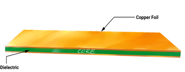
5.1 Use a Multi-Layer PCB
- Dedicated power and ground planes reduce impedance and noise coupling.
- Signal layers should be sandwiched between ground planes for shielding.
5.2 Implement Proper Decoupling
- Use a combination of bulk, ceramic, and high-frequency capacitors near power pins.
5.3 Minimize High-Frequency Current Paths
- Keep switching loops tight and use Kelvin connections for sensitive components.
5.4 Apply EMI Filters
- Pi-filters and ferrite beads help attenuate high-frequency noise.
5.5 Follow Regulatory Guidelines
- Adhere to standards like CISPR 32, FCC Part 15, and IEC 61000 for compliance.
6. Conclusion
The power supply layout significantly impacts a system’s EMC performance. By optimizing grounding, component placement, trace routing, and filtering, designers can reduce EMI and improve immunity. Following best practices ensures compliance with regulatory standards and enhances overall system reliability. Future advancements in PCB materials and simulation tools will further aid in achieving better EMC performance in power supply designs.