The Role and Importance of PCB CAM in Modern Electronics Manufacturing
Introduction to PCB CAM
Printed Circuit Board (PCB) Computer-Aided Manufacturing (CAM) represents a critical bridge between PCB design and physical production in the electronics manufacturing process. As electronic devices become increasingly complex while product lifecycles shrink, PCB CAM has evolved from a simple translation tool to a sophisticated system that ensures design integrity, manufacturing feasibility, and optimal production efficiency.
This article explores the multifaceted world of PCB CAM, examining its fundamental processes, technological advancements, industry applications, and future directions in electronics manufacturing.
Understanding PCB CAM Fundamentals
Definition and Core Functions
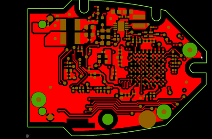
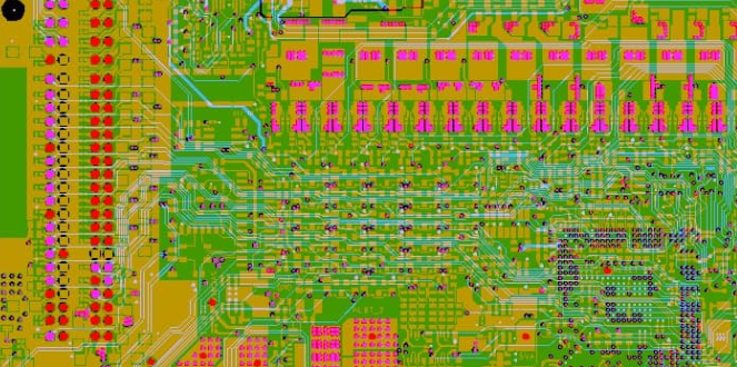
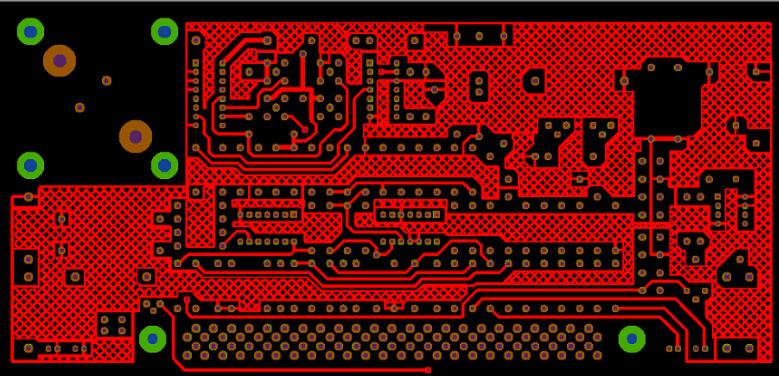
PCB CAM refers to the specialized software and processes that convert PCB design data (typically from CAD systems) into manufacturing instructions for PCB fabrication and assembly. The CAM system acts as the critical intermediary that ensures the designer’s intent is accurately translated into a physical product while accounting for all manufacturing constraints.
The core functions of PCB CAM include:
- Design data import and verification
- Manufacturing rule checks (beyond design rule checks)
- Panelization and array creation
- Toolpath generation for drilling and routing
- Photoplot file generation (Gerber, ODB++, etc.)
- Documentation creation for the entire manufacturing process
The CAM Workflow
A typical PCB CAM workflow progresses through several distinct stages:
- Data Import: Receiving design files in various formats (Gerber, ODB++, IPC-2581, CAD native formats)
- Data Verification: Ensuring all layers align properly and contain no design flaws
- Manufacturing Preparation: Adjusting designs for producibility (compensating for etching, plating, etc.)
- Panelization: Arranging multiple PCBs on a production panel for efficient manufacturing
- Tooling Generation: Creating files for drilling, routing, and other machining operations
- Output Generation: Producing all necessary files for fabrication and assembly
Advanced PCB CAM Technologies
Intelligent DFM Analysis
Modern PCB CAM systems incorporate sophisticated Design for Manufacturability (DFM) analysis that goes far beyond basic design rule checking. These systems can:
- Predict and compensate for manufacturing distortions (etch compensation, copper balancing)
- Analyze drill-to-copper relationships for reliability
- Verify impedance control structures
- Evaluate plating uniformity concerns
- Assess solder mask registration tolerances
Automated Panelization Systems
Advanced panelization features now include:
- Intelligent breakout tab placement for different board types
- Automatic fiducial and tooling hole placement
- Mixed technology panels (combining different PCB types)
- Dynamic spacing adjustment based on material characteristics
- 3D panel visualization for complex assemblies
Direct CAD-CAM Integration
Leading CAM solutions now offer tight integration with PCB CAD systems, enabling:
- Bi-directional data exchange
- Real-time design updates in the CAM environment
- Shared design rules and constraints
- Collaborative review processes between design and manufacturing teams
Industry Applications
High-Density Interconnect (HDI) PCBs
PCB CAM plays a particularly crucial role in HDI manufacturing, where:
- Microvia formation and stacking requires precise registration
- Laser drilling parameters must be carefully controlled
- Sequential lamination processes demand exact layer-to-layer alignment
- Thin dielectric materials require special handling considerations
Flexible and Rigid-Flex Circuits
For flexible PCB technologies, CAM systems must account for:
- Dynamic flex areas and bend radius requirements
- Coverlay openings and adhesive flows
- Stiffener placement and material interactions
- Dimensional stability during processing
RF/Microwave PCBs
High-frequency designs present unique CAM challenges:
- Critical impedance control on curved traces
- Precise dielectric constant management
- Specialized plating requirements for RF performance
- Unique solder mask applications
The Future of PCB CAM
AI and Machine Learning Integration
Emerging technologies are transforming PCB CAM through:
- Predictive analytics for manufacturing yields
- Self-optimizing panelization algorithms
- Automated DFM recommendation engines
- Intelligent defect prediction systems
Industry 4.0 and Smart Manufacturing
PCB CAM is evolving into a central component of smart factories with:
- Real-time process adjustment based on manufacturing feedback
- Digital twin integration for virtual manufacturing
- Closed-loop quality control systems
- Automated process flow optimization
Advanced Materials Support
Future CAM systems will need to handle:
- Novel substrate materials (high-speed, high-frequency, thermal management)
- Additive manufacturing processes
- Embedded component technologies
- Sustainable and recyclable materials
Conclusion
PCB CAM has grown from a simple translation tool to become the central nervous system of PCB manufacturing, ensuring the seamless transition from design concept to physical product. As electronics continue their relentless advancement, PCB CAM systems will play an increasingly vital role in managing complexity, ensuring quality, and optimizing manufacturing efficiency.
The future of PCB CAM lies in smarter, more connected systems that leverage artificial intelligence, real-time data analytics, and deep manufacturing knowledge to push the boundaries of what’s possible in electronics manufacturing. Companies that invest in advanced CAM capabilities will gain significant competitive advantages in time-to-market, product quality, and manufacturing efficiency.
For PCB manufacturers and designers alike, understanding and leveraging the full potential of modern PCB CAM technology is no longer optional—it’s an essential requirement for success in today’s fast-paced, technology-driven marketplace.