The Role of Advanced PCBs in 5G Communication Systems
Introduction
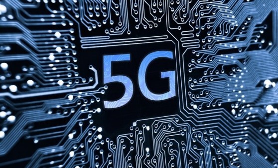
The rapid expansion of 5G technology is revolutionizing global communication, enabling faster data transfer, lower latency, and enhanced connectivity for IoT, autonomous vehicles, and smart cities. At the heart of 5G infrastructure lies the printed circuit board (PCB), which serves as the foundation for high-frequency signal transmission, power management, and thermal regulation.
As 5G operates at higher frequencies (mmWave bands up to 28 GHz and beyond), traditional PCB materials and designs are no longer sufficient. Instead, advanced high-frequency PCBs with superior signal integrity, thermal stability, and miniaturization capabilities are essential. This article explores the key challenges, materials, design considerations, and applications of 5G communication PCBs.
1. Key Challenges in 5G PCB Design
1.1 High-Frequency Signal Loss
5G networks rely on millimeter-wave (mmWave) frequencies, which introduce significant signal attenuation. To minimize loss, PCBs must use low-loss dielectric materials (e.g., PTFE, Rogers, or ceramic-filled laminates) instead of standard FR-4.
1.2 Impedance Control & Signal Integrity
High-speed signals in 5G require strict impedance control (typically 50Ω or 100Ω differential). Any mismatch can cause reflections, leading to data errors. Controlled dielectric constants (Dk) and dissipation factors (Df) are crucial for maintaining signal integrity.
1.3 Heat Dissipation & Thermal Management
5G PCBs generate more heat due to higher power amplifiers and dense circuitry. Effective thermal vias, metal-core PCBs, and heat sinks are necessary to prevent overheating and ensure reliability.
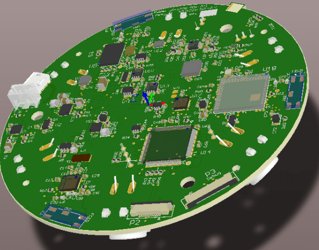
1.4 Miniaturization & High-Density Interconnect (HDI)
5G devices demand smaller, lighter PCBs with high-density interconnects (HDI). This requires microvias, stacked vias, and fine-pitch traces to accommodate complex RF and digital circuits in compact spaces.
2. Critical Materials for 5G PCBs
2.1 Low-Loss Substrates
- PTFE (Teflon): Excellent high-frequency performance but expensive.
- Rogers RO4000 Series: Popular for RF/microwave applications.
- Ceramic-Filled Laminates: Enhance thermal conductivity.
2.2 Copper Foil Selection
- Low-profile copper reduces skin effect losses at high frequencies.
- Reverse-treated copper (RTF) improves adhesion for fine-line etching.
2.3 Advanced Surface Finishes
- ENIG (Electroless Nickel Immersion Gold): Good for RF applications.
- OSP (Organic Solderability Preservative): Cost-effective but less durable.
- Immersion Silver: Low loss and suitable for high-frequency signals.
3. Design Considerations for 5G PCBs
3.1 RF & Mixed-Signal Layout Techniques
- Separate analog and digital grounds to reduce noise.
- Use coplanar waveguides for mmWave signal routing.
- Minimize via stubs to prevent signal reflections.
3.2 EMI/EMC Shielding
- Embedded shielding using conductive films or grounded copper.
- Faraday cage structures around sensitive RF components.
3.3 Power Integrity
- Low-impedance power distribution networks (PDNs) to minimize voltage drops.
- Decoupling capacitors near ICs to stabilize power supply.
4. Applications of 5G PCBs
4.1 5G Base Stations & Antennas
- Massive MIMO (Multiple Input Multiple Output) antennas require multi-layer RF PCBs with precise impedance control.
4.2 Smartphones & Mobile Devices
- Antenna-in-Package (AiP) and Antenna-on-PCB (AoP) designs for mmWave 5G.
4.3 Automotive & V2X Communication
- Vehicle-to-Everything (V2X) PCBs must withstand harsh environments while maintaining signal integrity.
4.4 IoT & Edge Computing
- Miniaturized 5G PCBs enable low-latency communication for smart sensors and AI-driven devices.
5. Future Trends in 5G PCB Technology
5.1 Integration with AI & Machine Learning
AI-driven automated PCB design tools optimize layouts for 5G performance.
5.2 3D-Printed & Embedded Components
- Additive manufacturing enables faster prototyping of high-frequency PCBs.
- Embedded passive/active components reduce size and improve efficiency.
5.3 Sustainable & High-Thermal PCBs
- Biodegradable substrates and lead-free soldering for eco-friendly PCBs.
- Advanced cooling solutions like liquid-cooled PCBs for high-power 5G systems.
Conclusion
5G communication PCBs are at the forefront of next-gen wireless technology, demanding advanced materials, precision engineering, and innovative thermal management. As 5G adoption grows, PCB manufacturers must continue evolving to meet the high-frequency, high-speed, and miniaturization requirements of modern networks.
By leveraging low-loss dielectrics, HDI techniques, and AI-driven design optimization, the PCB industry will play a pivotal role in shaping the future of 5G and beyond.


