The Structural Composition of PCB Circuit Boards
Introduction
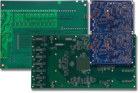
Printed Circuit Boards (PCBs) are the backbone of modern electronics, providing mechanical support and electrical connectivity for electronic components. Understanding the structure of a PCB is essential for engineers, designers, and anyone involved in electronics manufacturing. This article explores the key structural components of a PCB, including substrate materials, conductive layers, solder mask, silkscreen, and vias, while also discussing different types of PCBs and their applications.
1. Core Substrate Material
The foundation of any PCB is the substrate, which provides mechanical strength and insulation. The most common substrate materials include:
1.1 FR-4 (Flame Retardant-4)
- Made from woven fiberglass cloth with an epoxy resin binder.
- Offers excellent electrical insulation, mechanical rigidity, and flame resistance.
- Widely used in consumer electronics, industrial controls, and computing devices.
1.2 Flexible Substrates (Polyimide, PET)
- Used in flexible PCBs (FPCBs) for bendable applications.
- Common in wearables, medical devices, and aerospace electronics.
1.3 Metal Core PCBs (MCPCBs)
- Feature a metal base (usually aluminum or copper) for better heat dissipation.
- Used in LED lighting, power electronics, and automotive systems.
1.4 Ceramic Substrates
- Provide high thermal conductivity and stability.
- Used in high-frequency and high-power applications.
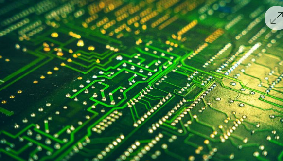
2. Conductive Layers (Copper Traces)
The conductive pathways on a PCB are made of copper, which is laminated onto the substrate. The number of conductive layers determines the PCB type:
2.1 Single-Layer PCBs
- One conductive layer (top or bottom).
- Simple and cost-effective, used in basic electronics like calculators and power supplies.
2.2 Double-Layer PCBs
- Conductive layers on both sides, connected by vias.
- Common in industrial controls, automotive dashboards, and IoT devices.
2.3 Multilayer PCBs (4+ Layers)
- Multiple conductive layers separated by insulating dielectric material.
- Used in high-speed digital circuits (motherboards, smartphones, servers).
2.4 High-Density Interconnect (HDI) PCBs
- Feature microvias and finer traces for compact designs.
- Essential for smartphones, tablets, and advanced medical devices.
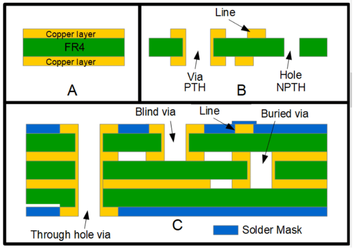
3. Dielectric Layers (Prepreg & Core)
The insulating layers between copper traces prevent short circuits and ensure signal integrity.
3.1 Core Material
- Rigid base material (e.g., FR-4) with copper layers pre-bonded on both sides.
3.2 Prepreg (Pre-Impregnated Fiberglass)
- Partially cured epoxy resin used to bond layers in multilayer PCBs.
- Becomes fully solid during the lamination process.

4. Solder Mask
The solder mask is a protective polymer coating applied over the copper traces to prevent oxidation and short circuits.
4.1 Functions of Solder Mask
- Prevents solder bridges during assembly.
- Protects copper from environmental damage (moisture, dust).
- Improves electrical insulation.
4.2 Common Colors
- Green (most common), red, blue, black, and white.
5. Silkscreen (Legend Printing)
The silkscreen layer adds text, symbols, and component identifiers to assist in assembly and debugging.
5.1 Typical Information Printed
- Component reference designators (R1, C2, U3).
- Polarity markers, pin-1 indicators, and logos.
5.2 Printing Methods
- Liquid Photo Imaging (LPI) for high precision.
- Inkjet printing for low-cost prototypes.
6. Vias: Electrical Connections Between Layers
Vias are conductive holes that connect different PCB layers.
6.1 Through-Hole Vias
- Drilled through the entire PCB, plated with copper.
- Used in most standard PCBs.
6.2 Blind and Buried Vias
- Blind vias connect an outer layer to an inner layer.
- Buried vias connect only inner layers (not visible from the outside).
- Used in HDI PCBs to save space.
6.3 Microvias
- Smaller than traditional vias (diameter < 150 µm).
- Essential for high-density designs like smartphones.
7. Surface Finishes
The exposed copper pads require a surface finish to prevent oxidation and improve solderability.
7.1 HASL (Hot Air Solder Leveling)
- Traditional finish with a tin-lead (or lead-free) coating.
- Cost-effective but not suitable for fine-pitch components.
7.2 ENIG (Electroless Nickel Immersion Gold)
- Provides a flat surface, excellent for fine-pitch and BGA components.
- Resistant to oxidation but more expensive.
7.3 OSP (Organic Solderability Preservative)
- A thin organic coating that protects copper until soldering.
- Low-cost but has a limited shelf life.
7.4 Immersion Silver & Tin
- Used as lead-free alternatives to HASL.
8. Additional PCB Features
8.1 Gold Fingers
- Gold-plated edge connectors for high-reliability contacts (e.g., RAM slots).
8.2 Stiffeners (for Flexible PCBs)
- Reinforce areas where components are mounted.
8.3 RF Shielding
- Metal cans or conductive coatings to prevent electromagnetic interference (EMI).
Conclusion
A PCB is a complex structure composed of multiple layers and materials, each serving a critical function in ensuring electrical performance, mechanical stability, and manufacturability. From the substrate and copper traces to the solder mask and vias, every element must be carefully designed to meet the demands of modern electronics. As technology advances, PCBs continue to evolve, enabling smaller, faster, and more reliable electronic devices.
Understanding PCB structure is essential for engineers to optimize designs, troubleshoot issues, and select the right materials for their applications. Whether designing a simple single-layer board or a high-speed multilayer HDI PCB, knowledge of these structural components is fundamental to success in electronics manufacturing.