The”Bridge Builder”of the Microscopic world:Unveiling the Secrets PCB soldering
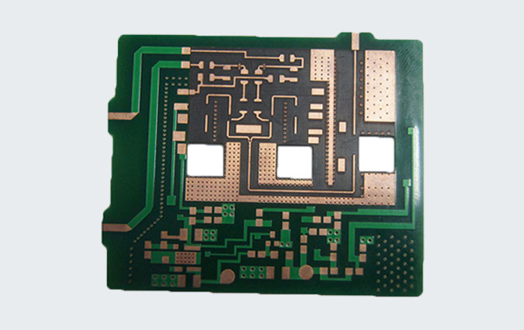
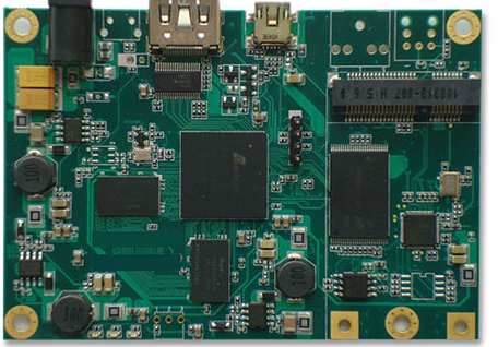
When you use your smartphone.operate a computer,or even flip on a smart light switch,have you ever wondered how these electronic devices:”think”and”work”internally?The answer lies on a board covered in silver lines and a myriad of components-this is the printed circuit board.The key process for firmly attaching these components to the board and establishing electrical connections is our topic today:PCB soldering.
1.What is soldering?It’s more Than just”sticks”
simply put ,soldering uses a solder with a lower melting point than the metals being joined.Heat causes it to melt,forming a strong,conductive alloy layer between the component pins and the PCB pads.
The key point is:
It’s not glue:soldering forms a metallurgical bond between metal atoms,resulting in excellent conductivity and a very strong connection
It’s a bridge:It acts as both a physical”anchor” to secure component and and electrical”highway”to allow current and signals to flow smoothly.Imagine building piers for a small bridge(component)between two opposite roads(conductors on a PCB).Soldering is the process of creating a sturdy,traffica-safe(conductive)pier.
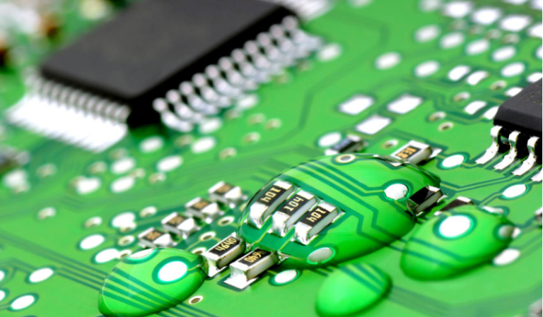
2.Core Materials:solder and Flux solder:The”Flesh and Blood”of soldering
Traditional solder wire:Its primary component is a tin-lead alloy(such as Sn63/Pb37),which has a low melting point and excellent soldering properties.However,due to the environmental and health hazards of lead,it is currently being phased out.
lead-free solder wire:The mainstream of modern electronics manufacturing,It is typically an alloy of tin,silver,and copper(such as SAC305,which is 96.5%tin,3%silver,and 0.5%copper).it has a slightly higher melting point but is more environmentally friendly.
Flux:The”God of Soldering”
solder often contains flux.Its functions are crucial:
Cleaning:It removes the oxide layer on the surface of the solder pads and component leads,providing a “bath”for the metal surfaces to be soldered.
Preventing reoxidation:It forms a protective film during heating to prevent reoxidation at high temperature.
Reducing surface tension:Helps the molten solder better”wet”and “spread”on the metal surface,forming a perfect meniscus shape.
3.Common Soldering Methods
Soldering methods vary depending on the application and scale
(1).Hand Soldering-The Art of the Craftsman
This is the most common and fundamental soldering method,and its core tool is the soldering iron.
Suitable for:Product development,repair,small-batch production,and DIY assembly.
Basic steps:
Preparation:Prepare the soldering iron,solder wick,component,and PCB.
Heating:Use the soldering iron tip to heat thr component pin and PCB pad simultaneously(approximately1-2seconds).
Feeding:Apply the solder wick to the contact point between the heated pin and the pad rather than directly onto the soldering iron tip.
Wetting:Observe the molten solder naturally soak into and surround the pad and pin,forming a smooth ,bright cone.
Removal:Remove the solder wick first,then quickly remove the soldering iron tip and allow the solder joint to cool naturally. soak into and surround the pad and pin,forming a smooth ,bright cone.
Challenges:Requires high operator skill,requiring precise control of temperature,time,and solder delivery.
(2)Reflow Oven-Mass production Tool
This is the primary method used in modern electronics factories to produce surface mount components such as mobile phone and computer motherboards
Application:large-scale soldering of surface mount components.
Basic Process
solder Paste printing:A stencil is used to precisely apply solder paste to PCB pads.
Component Placement:A placement machine precisely place tiny surface mount components(resistors,capacitor,chips)onto solder paste coated pad.
Reflow Oven:PCBs enter the reflow oven and pass through a precisely controlled temperature channer,undergoing four stages:preheating,constant temperature,reflow(melting),and cooling.In the reflow zone,the solder paste melts,and surface tension and flux automatically form perfect solder joints.
(3)Wave soldering-leaded component production line
Primarily used for soldering long lead plug-in components on the backside of PCBs.
Application:Mass soldering of through-hole components.
Process:The soldering surface of the PCB is exposed to “wave”of molten solder.The liquid solder surges upward,simulateneously soldering all pins,resulting in extremely high efficiency.
4.How to judge solder joint quality?
A perfect solder joint should have the following characteristic:
smooth and bright:The surface is as smooth as a mirrior and has a metallic luster.
Uniform shape:The solder smoothly connects the pad and pin,forming a concave surface with a small contact angle.
Suitable solder:The solder just covers the entire pad ,forming a good solder joint.