Thermal Relief in PCB Design: Importance, Design Considerations, and Best Practices
1. Introduction
Printed Circuit Boards (PCBs) are essential components in modern electronics, providing mechanical support and electrical connections for electronic components. One critical aspect of PCB design is managing heat dissipation, especially during soldering processes. Thermal relief is a design technique used to improve soldering quality and prevent heat-related issues in PCB manufacturing.
This article explores the concept of thermal relief in PCB design, its importance, design considerations, and best practices for implementation.
2. What is Thermal Relief?
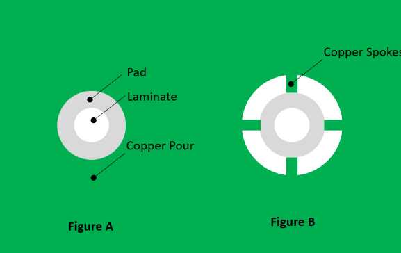
Thermal relief, also known as thermal pads or thermal spokes, refers to a specific pattern of traces or spokes connecting a pad to a copper plane (such as a ground or power plane) in a PCB. Unlike a direct solid connection, thermal relief uses narrow traces to reduce heat transfer while maintaining electrical conductivity.
2.1 Why is Thermal Relief Necessary?
During soldering (especially in wave soldering or reflow processes), excessive heat dissipation through large copper planes can lead to:
- Poor solder joint formation – If heat is drawn away too quickly, solder may not melt properly, resulting in cold joints.
- Difficulty in manual soldering – Technicians may struggle to heat pads sufficiently when connected directly to large copper areas.
- Thermal stress on components – Rapid heating and cooling cycles can damage sensitive components.
Thermal relief mitigates these issues by reducing the thermal mass connected to the pad, allowing for better heat retention during soldering.

3. Structure of Thermal Relief Pads
A typical thermal relief structure consists of:
- A central pad (where the component lead or via is placed).
- Thermal spokes (usually 2 to 4 thin traces connecting the pad to the copper plane).
- Isolation gaps (small breaks in the copper pour around the pad to limit heat transfer).
3.1 Common Thermal Relief Patterns
- Cross-Hair (4-Spoke) Design – Four thin traces at 90-degree angles (most common).
- 3-Spoke Design – Used when space is limited.
- Modified Spoke Shapes – Some designs use curved or wider spokes for better current handling.
4. Benefits of Using Thermal Relief in PCBs
4.1 Improved Soldering Quality
- Ensures proper solder reflow by preventing excessive heat dissipation.
- Reduces the risk of cold solder joints or tombstoning in surface-mount components.
4.2 Easier Rework and Repairs
- Allows easier desoldering and component replacement by reducing heat sinking effects.
4.3 Better Thermal Management
- Balances heat distribution during soldering while maintaining electrical performance.
4.4 Prevention of Copper Peeling
- Reduces thermal stress on copper planes, preventing delamination during soldering.
5. Design Considerations for Thermal Relief
5.1 When to Use Thermal Relief
- Through-hole components – Especially for pins connected to ground/power planes.
- High-power components – Where heat dissipation must be controlled.
- Wave soldering applications – To ensure uniform heating.
5.2 When to Avoid Thermal Relief
- High-current paths – Thicker direct connections may be needed to handle current without excessive resistance.
- RF and high-frequency circuits – Solid connections may be necessary to minimize impedance variations.
5.3 Key Design Parameters
- Spoke Width – Typically 10-20 mils (0.25-0.5 mm); wider spokes conduct more heat.
- Number of Spokes – Usually 2 to 4; more spokes increase heat transfer.
- Air Gap (Isolation) – The gap between the pad and the copper plane (typically 5-10 mils).
- Pad Size – Must match component lead size for proper soldering.
6. Thermal Relief in Different PCB Design Software
Most PCB design tools (such as Altium Designer, KiCad, Eagle, and OrCAD) include automated thermal relief generation. Here’s how they are typically implemented:
6.1 Altium Designer
- Configure thermal relief settings in Design > Rules > Plane > Polygon Connect Style.
- Options include Relief Connect, Direct Connect, and No Connect.
6.2 KiCad
- Set thermal relief in Edit > Pad Properties > Thermal Relief.
- Adjust spoke width and gap settings.
6.3 Eagle
- Defined in Design Rules (DRC) > Thermals tab.
- Customize spoke width and number.
6.4 OrCAD/Allegro
- Configure in Shape > Global Dynamic Shape Parameters > Thermal Relief Connects.
7. Common Mistakes in Thermal Relief Design
- Insufficient Spoke Width – Too narrow spokes can break during soldering.
- Excessive Spokes – Too many spokes defeat the purpose by increasing heat transfer.
- Incorrect Air Gap – Too small a gap reduces thermal relief effectiveness.
- Missing Thermal Relief on Ground Planes – Leads to soldering difficulties.
- Overusing Thermal Relief in High-Current Paths – Causes excessive resistance and heating.
8. Best Practices for Implementing Thermal Relief
- Follow Manufacturer Guidelines – Check PCB fabrication house recommendations.
- Optimize Spoke Width and Count – Balance heat retention and electrical conductivity.
- Use Symmetrical Spokes – Ensures even heat distribution.
- Review High-Current Paths – Avoid thermal relief where low resistance is critical.
- Test Prototypes – Verify soldering performance before mass production.
9. Conclusion
Thermal relief is a crucial aspect of PCB design that enhances soldering quality, improves manufacturability, and prevents heat-related defects. By understanding its structure, benefits, and design considerations, engineers can optimize their PCBs for both performance and reliability.
Proper implementation in PCB design software, along with adherence to best practices, ensures robust thermal management without compromising electrical integrity. As PCB technology evolves, thermal relief techniques will continue to play a vital role in high-quality electronic manufacturing.


