Thin Film PCB: Revolutionizing Modern Electronics
Introduction
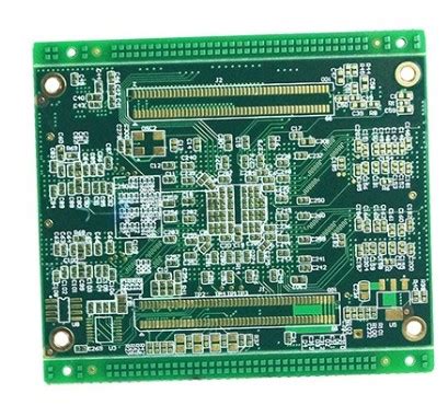
Printed Circuit Boards (PCBs) are the backbone of modern electronics, providing the necessary platform for interconnecting electronic components. As technology advances, the demand for more compact, efficient, and high-performance electronic devices has led to the development of Thin Film PCBs. These specialized PCBs offer numerous advantages over traditional thick film and rigid PCBs, making them indispensable in applications ranging from consumer electronics to aerospace and medical devices. This article delves into the intricacies of Thin Film PCBs, exploring their manufacturing processes, advantages, applications, and future prospects.
What is a Thin Film PCB?
A Thin Film PCB is a type of printed circuit board that utilizes thin layers of conductive and insulating materials, typically deposited on a substrate using advanced techniques such as sputtering, evaporation, or chemical vapor deposition (CVD). The thickness of these layers is usually in the range of a few micrometers, significantly thinner than the layers found in traditional thick film PCBs. This thinness allows for greater precision, higher density of components, and improved electrical performance.

Manufacturing Process of Thin Film PCBs
The manufacturing process of Thin Film PCBs is highly specialized and involves several precise steps:
- Substrate Preparation: The process begins with the selection and preparation of a suitable substrate. Common materials include ceramics, glass, and flexible polymers like polyimide. The substrate must be meticulously cleaned to ensure proper adhesion of the thin film layers.
- Deposition of Conductive Layers: Thin layers of conductive materials, such as copper, gold, or aluminum, are deposited onto the substrate using techniques like sputtering or evaporation. These methods allow for the creation of extremely thin and uniform conductive layers, which are essential for high-performance circuits.
- Patterning: The conductive layers are then patterned to form the desired circuit layout. This is typically achieved through photolithography, where a photoresist is applied, exposed to UV light through a mask, and developed to create the circuit pattern. The exposed areas are then etched away, leaving behind the conductive traces.
- Deposition of Insulating Layers: Insulating layers, often made of materials like silicon dioxide or polyimide, are deposited over the conductive traces to provide electrical isolation. These layers are also very thin, ensuring minimal impact on the overall thickness of the PCB.
- Via Formation: Vias are small holes drilled through the insulating layers to create electrical connections between different layers of the PCB. These vias are then filled with conductive material to establish the necessary interconnections.
- Surface Finishing: The final step involves applying surface finishes to protect the conductive traces and improve solderability. Common finishes include gold plating, solder mask application, and organic solderability preservatives (OSPs).

Advantages of Thin Film PCBs
Thin Film PCBs offer several advantages over traditional PCBs, making them ideal for a wide range of applications:
- High Precision and Miniaturization: The thin layers and precise deposition techniques allow for the creation of highly detailed and compact circuits. This is particularly beneficial in applications where space is at a premium, such as in mobile devices and wearable electronics.
- Improved Electrical Performance: The thin conductive layers reduce parasitic capacitance and inductance, leading to better signal integrity and higher frequency performance. This makes Thin Film PCBs suitable for high-speed and RF applications.
- Flexibility: Thin Film PCBs can be fabricated on flexible substrates, enabling the creation of flexible and bendable circuits. This is advantageous in applications like flexible displays, medical devices, and automotive electronics.
- Thermal Management: The thin layers and high thermal conductivity of materials used in Thin Film PCBs facilitate efficient heat dissipation, which is crucial in high-power applications.
- Lightweight: The reduced thickness and weight of Thin Film PCBs make them ideal for aerospace and portable electronics, where weight savings are critical.
- Durability: Thin Film PCBs are often more durable than traditional PCBs, with better resistance to environmental factors like moisture, temperature fluctuations, and mechanical stress.
Applications of Thin Film PCBs
The unique properties of Thin Film PCBs have led to their adoption in a wide range of industries and applications:
- Consumer Electronics: Thin Film PCBs are widely used in smartphones, tablets, and wearable devices, where their compact size and high performance are essential. They enable the integration of complex circuits into small form factors, contributing to the sleek and lightweight designs of modern gadgets.
- Medical Devices: In the medical field, Thin Film PCBs are used in devices like pacemakers, hearing aids, and diagnostic equipment. Their flexibility and reliability are crucial in these life-saving applications.
- Aerospace and Defense: The aerospace and defense industries benefit from the lightweight and durable nature of Thin Film PCBs. They are used in avionics, satellites, and military communication systems, where performance and reliability are paramount.
- Automotive Electronics: Thin Film PCBs are increasingly used in automotive applications, including advanced driver-assistance systems (ADAS), infotainment systems, and engine control units. Their ability to withstand harsh environments and high temperatures makes them ideal for these applications.
- Industrial Electronics: In industrial settings, Thin Film PCBs are used in automation systems, sensors, and control units. Their high precision and reliability contribute to the efficiency and safety of industrial processes.
- Telecommunications: The high-frequency performance of Thin Film PCBs makes them suitable for telecommunications equipment, including routers, switches, and base stations. They enable the transmission of high-speed data with minimal signal loss.

Challenges and Future Prospects
Despite their numerous advantages, Thin Film PCBs also present certain challenges:
- Cost: The specialized manufacturing processes and materials used in Thin Film PCBs can result in higher costs compared to traditional PCBs. However, as technology advances and economies of scale are achieved, these costs are expected to decrease.
- Complexity: The fabrication of Thin Film PCBs requires advanced equipment and expertise, which can be a barrier to entry for some manufacturers. Ongoing research and development are focused on simplifying the manufacturing process and making it more accessible.
- Material Limitations: The choice of materials for Thin Film PCBs is somewhat limited, particularly for flexible substrates. Researchers are exploring new materials and deposition techniques to expand the range of options and improve performance.
Looking ahead, the future of Thin Film PCBs is promising. Advances in materials science, nanotechnology, and manufacturing techniques are expected to further enhance the performance and reduce the cost of Thin Film PCBs. Emerging applications in areas like Internet of Things (IoT), 5G telecommunications, and renewable energy are likely to drive demand for these advanced PCBs.
Conclusion
Thin Film PCBs represent a significant advancement in the field of printed circuit boards, offering unparalleled precision, performance, and flexibility. Their unique properties make them indispensable in a wide range of applications, from consumer electronics to aerospace and medical devices. While challenges remain, ongoing research and development are paving the way for even greater innovations in Thin Film PCB technology. As the demand for smaller, faster, and more reliable electronic devices continues to grow, Thin Film PCBs will undoubtedly play a crucial role in shaping the future of electronics.


