Through Hole PCB Assembly: Key Benefits and Implementation Strategies

Key Takeaways
When considering PCB assembly methodologies, through-hole technology (THT) remains a cornerstone for applications demanding enhanced mechanical stability and long-term reliability. Below are critical insights to guide decision-making:
- Durability Advantages: Through-hole components form physical bonds with the board, making them ideal for high-stress environments. This is particularly valuable in aerospace or industrial equipment where PCBA integrity is non-negotiable.
- Design Flexibility: Unlike surface-mount devices (SMDs), through-hole parts allow easier manual adjustments, simplifying prototyping and low-volume PCB assembly runs.
- Thermal Resilience: The extended lead-to-board contact in THT improves heat dissipation, reducing failure risks in power-intensive circuits.
"Through-hole assembly isn’t just about legacy systems—it’s a strategic choice for applications where robustness trumps miniaturization."
— Senior Engineer, Tier-1 Electronics Manufacturer
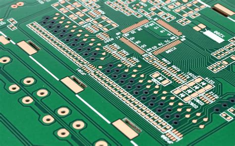
Comparative Analysis: Through-Hole vs. Surface Mount
| Factor | Through-Hole Assembly | Surface Mount Technology (SMT) |
|---|---|---|
| Mechanical Strength | High (leads penetrate board) | Moderate (surface adhesion) |
| Thermal Performance | Superior heat dissipation | Requires thermal vias/pads |
| Repairability | Easier component replacement | Complex rework processes |
Implementation Tip: For hybrid designs (combining THT and SMT), prioritize component placement to avoid shadowing effects during wave soldering. Place taller through-hole parts downstream of the solder flow to prevent interference with smaller SMDs.
Quality Assurance Considerations
- Automated Optical Inspection (AOI): Critical for verifying solder fillet integrity in PCBA workflows.
- Stress Testing: Simulate vibration and thermal cycling to validate through-hole joint durability.
By aligning PCB assembly strategies with these takeaways, manufacturers can optimize both performance and longevity in electronic systems.
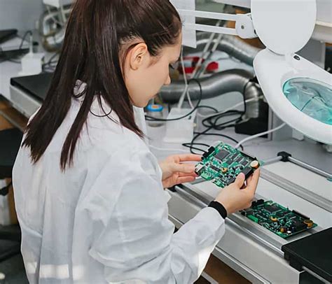
Through Hole PCB Assembly Process Overview
The PCB assembly process for through-hole technology (THT) involves a sequence of carefully orchestrated steps designed to ensure mechanical stability and electrical connectivity. Unlike surface-mount alternatives, this method relies on inserting component leads through pre-drilled holes in the board, creating robust physical bonds ideal for high-stress environments. The workflow typically begins with component preparation, where axial or radial leads are trimmed and formed to fit specific hole patterns.
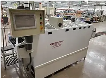
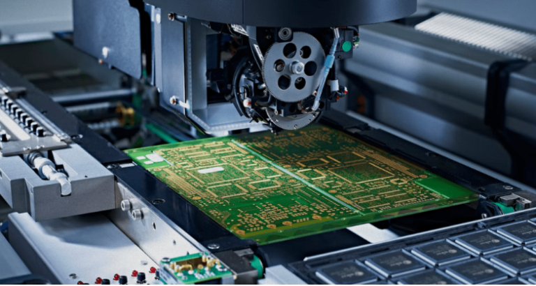
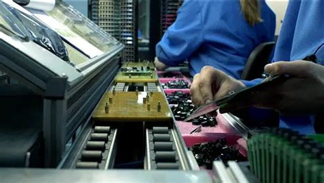
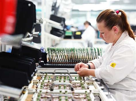
Automated insertion machines or manual placement techniques then position components onto the board, guided by design specifications. For mixed-technology boards requiring both PCBA (printed circuit board assembly) approaches, through-hole components are often placed after surface-mount devices to avoid thermal interference during soldering. The soldering phase employs wave soldering systems, where the board passes over a molten solder wave, uniformly coating leads and pads to form reliable connections. This process is particularly effective for high-volume production, though selective soldering may be used for heat-sensitive components.
Critical to the process is thermal management, as excessive heat can compromise substrate integrity. Post-soldering, boards undergo rigorous inspection using automated optical inspection (AOI) or X-ray imaging to detect defects like cold joints or misalignments. For applications demanding extreme reliability—such as aerospace or industrial controls—additional conformal coating may be applied to protect against environmental stressors.
By integrating precision drilling, controlled soldering, and multi-stage quality checks, through-hole PCB assembly balances durability with functional performance. This approach remains indispensable for applications where mechanical resilience and long-term reliability outweigh the need for miniaturization, ensuring its continued relevance in modern PCBA workflows.
Key Advantages of Through Hole Technology
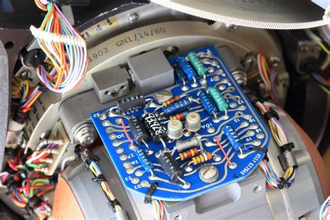
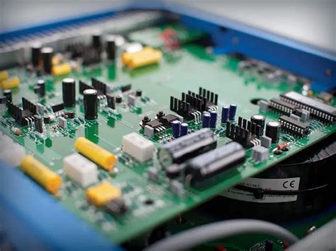
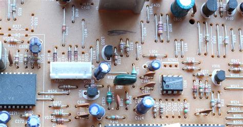
Through hole PCB assembly remains a cornerstone of electronic manufacturing, particularly for applications demanding mechanical stability and long-term reliability. Unlike surface-mount alternatives, through hole technology (THT) creates robust physical bonds by inserting component leads into pre-drilled holes, which are then soldered to form permanent connections. This method excels in environments subject to high vibration, thermal stress, or mechanical wear, making it indispensable for automotive, industrial, and aerospace PCBA designs.
One critical benefit lies in its superior load-bearing capacity. Components like connectors, transformers, and large capacitors benefit from the added structural integrity provided by through hole mounting. This durability reduces failure rates in devices exposed to repetitive physical stress, a key consideration for PCB assembly targeting mission-critical systems. Additionally, THT supports easier manual adjustments during prototyping, offering engineers greater flexibility in design validation and functional testing phases.
Thermal and electrical performance further distinguish through hole PCBA. The extended lead-to-board contact area enhances heat dissipation, improving reliability in power-intensive circuits. For high-voltage applications, the through hole process minimizes arcing risks by maintaining consistent spacing between conductive elements—a feature less reliably achieved with surface-mount technology.
Modern PCB assembly services leverage hybrid approaches, combining THT with automated soldering techniques to optimize efficiency. Wave soldering, for instance, ensures uniform joint formation across multi-layer boards while maintaining thermal tolerance thresholds. This synergy between traditional through hole methods and advanced manufacturing workflows underscores its enduring relevance in producing high-reliability electronics.
Finally, the technology’s compatibility with legacy components simplifies upgrades for industrial equipment, reducing redesign costs. As quality control standards tighten, through hole PCB assembly continues to serve as a benchmark for durability testing, with automated optical inspection (AOI) systems verifying solder fillet integrity to IPC-A-610 specifications. These advantages collectively position THT as a strategic choice for applications where failure is not an option.
Optimizing Component Placement Strategies
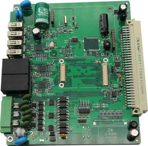
Effective PCB assembly relies on precise component placement to balance electrical performance, manufacturability, and long-term reliability. In through-hole PCBA, strategic positioning begins with analyzing thermal profiles and mechanical stress points. Components requiring higher structural integrity, such as connectors or transformers, should be placed near board edges or mounting holes to minimize vibration-induced failures. For mixed-technology boards, grouping through-hole parts in zones separated from surface-mount devices reduces soldering complexity and improves wave soldering efficiency.
Critical to this process is maintaining adequate spacing between components. A minimum clearance of 2.5 mm between adjacent through-hole leads prevents solder bridging while accommodating manual adjustments during prototyping. Orientation consistency—aligning polarized components like electrolytic capacitors in uniform directions—streamlines both automated and visual inspections. Advanced design-for-manufacturing (DFM) software now simulates heat dissipation patterns and pin accessibility, enabling engineers to preemptively address hotspots or assembly bottlenecks.
Transitioning from design to production, manufacturers often employ sequential placement protocols. High-power components are prioritized in areas with optimized airflow, while sensitive analog circuits are isolated from digital noise sources. This approach not only enhances PCBA performance but also reduces post-assembly rework rates by up to 40%, according to industry studies. For multi-layer boards, through-hole parts serving as structural anchors should avoid overlapping with internal signal layers to prevent impedance mismatches.
Finally, component height management ensures compatibility with enclosures and test fixtures. Tall elements like heat sinks or vertical connectors are positioned to avoid shadowing effects during conformal coating processes. By integrating these strategies, PCB assembly services achieve a balance between durability objectives and cost-effective scalability—a vital consideration for industrial and automotive applications where through-hole technology remains indispensable.
Advanced Soldering Techniques for Durability
Modern PCB assembly processes demand precision in soldering to ensure long-term reliability, particularly for through-hole components that endure mechanical stress in demanding applications. While automated wave soldering remains a cornerstone for high-volume production, specialized techniques like selective soldering enable targeted heat application for mixed-technology boards containing both through-hole and surface-mount devices. For mission-critical PCBA projects, hand soldering with temperature-controlled irons provides unparalleled control over joint formation, especially when working with heat-sensitive components or legacy parts requiring rework.
Material selection significantly impacts durability: lead-based solders (Sn63/Pb37) offer superior thermal fatigue resistance compared to lead-free alternatives, though RoHS compliance often mandates SAC305 alloys. To mitigate thermal stress, preheating stages in PCB assembly workflows gradually elevate board temperatures, minimizing sudden expansion mismatches between copper traces and substrate materials. Post-soldering, conformal coating applications create protective barriers against environmental factors like humidity and chemical exposure—a critical enhancement for industrial or automotive PCBA implementations.
Advanced inspection methodologies, including automated optical inspection (AOI) and X-ray imaging, validate solder joint integrity before proceeding to quality control phases. For through-hole connections, solder wicking prevention techniques—such as optimized dwell times and nitrogen-assisted soldering environments—ensure proper fillet formation without compromising adjacent components. As miniaturization trends push the limits of traditional PCB assembly, hybrid approaches combining robotic precision with artisan-grade process tuning are redefining durability standards for next-generation electronics manufacturing.
Quality Control in PCB Assembly Services
Effective PCB assembly processes require rigorous quality control measures to ensure the reliability of through-hole components in demanding applications. Modern PCBA providers implement multi-stage inspection protocols, beginning with automated optical inspection (AOI) systems that detect soldering defects, misaligned components, and pad irregularities at 5–10 μm resolution. For through-hole designs, X-ray inspection becomes critical to verify barrel fill rates in plated through-holes, ensuring 75–100% solder penetration as per IPC-A-610 Class 3 standards.
Material verification forms another cornerstone, with certified laboratories conducting cross-sectional analysis on 2% of production batches. This destructive testing method validates solder joint integrity, particularly for high-stress connections in industrial or automotive PCB assembly projects. Thermal cycle testing further assesses component endurance, subjecting boards to −40°C to +125°C transitions to simulate decade-long operational stresses within accelerated timelines.
Process control in PCBA manufacturing extends to solder bath management, where temperature fluctuations are maintained within ±2°C to prevent cold joints or thermal damage. Statistical process control (SPC) dashboards track 15+ parameters in real time, including wave solder contact duration (3–5 seconds optimal) and flux density (0.80–0.82 g/cm³ range). These metrics enable corrective adjustments before defects propagate, reducing rework rates below 0.8% in tier-1 facilities.
For mission-critical applications, environmental stress screening (ESS) protocols expose assembled boards to combined vibration (5–500 Hz) and humidity (85% RH) cycles. This preemptive approach identifies latent failures, improving mean time between failures (MTBF) by 18–22% compared to conventional testing methods. As through-hole technology evolves with mixed-technology designs, advanced PCB assembly services now integrate machine learning algorithms that analyze 10,000+ historical defect patterns to predict and prevent quality deviations.
Certified PCBA partners maintain traceability through blockchain-enabled documentation systems, recording component lot numbers, solder profiles, and inspection results for each production batch. This approach not only complies with ISO 9001:2015 requirements but also enables root cause analysis within 4–6 hours when field issues emerge—a 65% improvement over traditional paper-based systems.
Comparing Through Hole and Surface Mount
When selecting a PCB assembly methodology, engineers must weigh the distinct characteristics of through-hole technology (THT) and surface-mount technology (SMT). While PCBA workflows often integrate both approaches, understanding their core differences ensures optimal design and performance.
Mechanical strength remains a hallmark of through-hole components, as leads inserted into plated holes create robust physical connections. This makes THT ideal for connectors, transformers, or parts exposed to mechanical stress or high-temperature environments. In contrast, SMT components solder directly to surface pads, enabling high-density layouts and reduced board space—critical for compact devices like smartphones or wearables.
Thermal performance further distinguishes these methods. Through-hole soldering’s wave soldering compatibility ensures reliable joints for larger components, while SMT’s reflow oven processes achieve precise solder paste control for miniaturized parts. However, SMT’s smaller solder joints may exhibit lower vibration resistance compared to through-hole’s penetrative connections.
Cost considerations reveal another trade-off: SMT’s automated placement slashes labor expenses for high-volume production, whereas through-hole assembly often requires manual intervention for component insertion or inspection. Despite this, industries requiring extreme reliability—such as aerospace or industrial controls—frequently prioritize THT’s proven durability over SMT’s cost savings.
Modern PCB assembly services increasingly adopt hybrid strategies, leveraging SMT for high-speed signal paths and THT for power delivery sections. This approach balances manufacturing efficiency with performance requirements, ensuring boards meet both electrical and mechanical demands.
As component miniaturization advances, the role of through-hole technology evolves rather than diminishes. Its continued relevance in mission-critical applications underscores the importance of selecting assembly methods based on functional priorities rather than industry trends alone.
Implementing Reliable PCB Testing Methods
Effective testing protocols form the backbone of quality assurance in PCB assembly processes. For through-hole technology applications, where mechanical stability and long-term reliability are critical, implementing multi-stage testing strategies ensures defects are identified early. In-circuit testing (ICT) remains a cornerstone method, validating electrical connectivity and component functionality by applying test probes to predefined contact points. This approach is particularly effective for PCBA units with complex through-hole configurations, as it verifies solder joint integrity and pin alignment under simulated operational conditions.
Advanced manufacturers now integrate automated optical inspection (AOI) systems to complement traditional testing. These high-resolution cameras detect microscopic soldering flaws, such as insufficient fill in plated through-holes or tombstoning effects, which manual inspections might miss. When combined with PCB assembly process controls, AOI reduces post-production rework rates by up to 67%, according to industry benchmarks.
For mission-critical applications, functional testing simulates real-world operating environments to stress-test assembled boards. This phase often involves thermal cycling assessments to evaluate through-hole components’ resilience to expansion-contraction forces—a vital step given the technology’s prevalence in automotive and industrial electronics.
To maintain consistency, leading PCBA providers employ statistical process control (SPC) tools that correlate testing data with production parameters. For example, variations in wave soldering temperatures identified during ICT can trigger immediate adjustments in upstream processes, creating a closed-loop quality ecosystem. This proactive alignment between testing and manufacturing stages not only enhances product reliability but also aligns with evolving industry standards for traceability and compliance.
Transitioning to next-generation solutions, some assemblers now embed boundary-scan testing capabilities into through-hole designs. This technique allows ongoing performance monitoring without physical probes, significantly accelerating validation cycles for high-density boards while preserving the mechanical advantages of through-hole mounting.
Future Trends in Through Hole Assembly
While surface mount technology (SMT) dominates modern PCB assembly, through-hole techniques continue to evolve, adapting to emerging demands in specialized industries. One significant trend is the integration of hybrid manufacturing approaches, combining PCBA processes with automated through-hole insertion systems. This fusion enables manufacturers to leverage the mechanical strength of through-hole components while maintaining the density advantages of SMT, particularly in aerospace and industrial control systems where vibration resistance is critical.
Advancements in robotic soldering and precision placement systems are streamlining through-hole workflows, reducing manual intervention without compromising the reliability that defines this technology. For instance, vision-guided robots now achieve micron-level accuracy in component alignment, ensuring optimal PCB assembly quality even for complex multi-layer boards. Additionally, the shift toward lead-free soldering alloys with higher thermal stability is addressing environmental regulations while enhancing joint durability under extreme operating conditions.
Another emerging trend is the adoption of smart manufacturing frameworks in PCBA production. IoT-enabled assembly lines now monitor solder bath temperatures and insertion forces in real time, using predictive analytics to preempt defects. This data-driven approach aligns with industry 4.0 standards, enabling adaptive process optimization for mixed-technology boards. Furthermore, material innovations like high-temperature substrates and reinforced through-hole platings are extending the lifespan of assemblies in automotive and renewable energy applications, where thermal cycling stresses are unavoidable.
As miniaturization pressures grow, through-hole technology is responding with micro-via enhancements and laser-drilled plating techniques, allowing finer pitch components without sacrificing mechanical integrity. These developments position through-hole PCB assembly as a complementary—rather than competing—solution in next-generation electronics, particularly for prototyping and low-volume, high-reliability applications.
Conclusion
The enduring relevance of through hole PCB assembly in modern electronics stems from its unique ability to balance mechanical stability with electrical performance. While surface mount technology dominates high-density applications, PCBA solutions leveraging through hole components continue to excel in scenarios demanding extreme durability and high-power handling. Manufacturers implementing this approach benefit from proven solder joint integrity, particularly in environments subject to vibration or thermal stress.
Strategic adoption of PCB assembly workflows requires aligning component selection with operational requirements—through hole parts remain indispensable for connectors, transformers, and large capacitors. Recent advancements in selective wave soldering and automated insertion systems have bridged efficiency gaps, enabling cost-effective production without compromising the mechanical anchoring advantages inherent to the technology.
Quality assurance protocols for PCBA projects must account for the specific challenges of through hole implementations, including barrel fill verification and lead protrusion control. As industries increasingly demand hybrid assemblies combining both through hole and surface-mount components, manufacturers that master mixed-technology integration will gain competitive advantages in aerospace, automotive, and industrial control markets.
The evolution of PCB assembly standards continues to validate through hole technology’s role in mission-critical systems, particularly when paired with modern automated optical inspection (AOI) and functional testing methodologies. Moving forward, the technology’s survival hinges on strategic adaptation to miniaturization trends while maintaining its core strengths in reliability-driven applications.
Frequently Asked Questions
What distinguishes through-hole technology from surface mount in PCB assembly?
Through-hole technology (THT) involves inserting component leads into drilled holes on the PCB, which are then soldered for secure connections. This contrasts with surface mount technology (SMT), where components are placed directly onto the board’s surface. Durability and mechanical stability make through-hole PCB assembly preferable for high-stress applications, while SMT excels in compact, high-density designs.
How does component placement affect through-hole assembly quality?
Strategic component placement minimizes signal interference and thermal stress during soldering. Proper spacing ensures efficient heat distribution during wave soldering, reducing risks of cold joints or component damage. PCBA manufacturers often use automated optical inspection (AOI) systems to verify alignment accuracy before soldering.
What soldering techniques enhance durability in through-hole PCB assembly?
Wave soldering remains the primary method, submerging the board’s underside in molten solder to create robust joints. For mixed-technology boards (combining THT and SMT), selective soldering targets specific through-hole components. Applying conformal coating post-soldering further protects against environmental factors like moisture or dust.
Why is quality control critical in through-hole PCB assembly services?
Rigorous testing—including in-circuit testing (ICT) and functional testing—ensures electrical performance and detects defects like solder bridges or open circuits. PCB assembly providers leverage X-ray inspection to examine hidden joints, ensuring compliance with industry standards such as IPC-A-610.
Are through-hole components more expensive than surface-mount alternatives?
While through-hole components often have higher material and labor costs due to manual insertion and drilling, their long-term reliability in harsh environments justifies the investment for applications like industrial equipment or aerospace systems.
What future trends are shaping through-hole assembly processes?
Hybrid designs integrating THT and SMT are gaining traction, balancing durability with miniaturization demands. Advances in automated insertion systems and lead-free solder alloys are also streamlining PCBA workflows while meeting eco-friendly regulations.
Ready to Optimize Your Through-Hole PCB Assembly?
For tailored solutions that prioritize reliability and performance, explore our comprehensive PCB assembly services. Click here to learn more about our capabilities or request a customized quote today.