Tin Spray PCB: A Comprehensive Guide to Surface Finishing Technology
1. Introduction
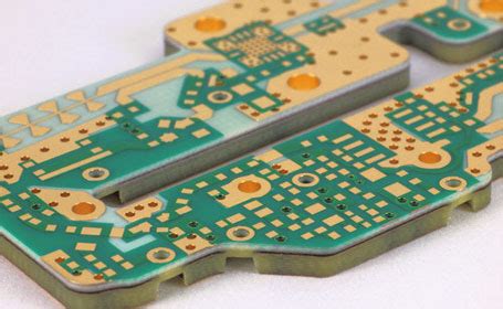
Printed Circuit Boards (PCBs) are the backbone of modern electronics, providing mechanical support and electrical connections for electronic components. One critical aspect of PCB manufacturing is surface finishing, which ensures solderability, corrosion resistance, and electrical conductivity. Among the various surface finishing techniques, Tin Spray (Hot Air Solder Leveling, HASL with Pure Tin) is a widely used method due to its cost-effectiveness and reliability.
This article explores Tin Spray PCB technology, discussing its process, advantages, disadvantages, applications, and comparisons with other surface finishes.
2. What is Tin Spray PCB?
Tin Spray, also known as Hot Air Solder Leveling (HASL) with Pure Tin, is a surface finishing process where molten tin (or tin-lead alloy in traditional HASL) is applied to the copper traces of a PCB. The board is then passed through hot air knives to level the coating and remove excess solder.
Unlike traditional Lead-based HASL, which uses a tin-lead alloy, Tin Spray PCB employs pure tin (Sn) to comply with RoHS (Restriction of Hazardous Substances) regulations, making it environmentally friendly.
Key Characteristics of Tin Spray PCB:
- Material: Pure Tin (Sn) or Tin-based alloy
- Thickness: Typically 1-40μm
- Process Temperature: ~250°C
- Compatibility: RoHS-compliant
3. The Tin Spray PCB Manufacturing Process
The Tin Spray process involves several steps:
Step 1: PCB Cleaning
- The bare copper PCB is cleaned to remove oxides, dust, and contaminants using chemical cleaning agents.
Step 2: Flux Application
- A flux is applied to improve solder wettability and prevent oxidation during the tin coating process.
Step 3: Tin Immersion or Spraying
- The PCB is dipped into a molten tin bath or sprayed with liquid tin to coat the exposed copper surfaces.
Step 4: Hot Air Leveling (HASL)
- The PCB passes through hot air knives, which blow off excess tin and create a smooth, even surface.
Step 5: Cooling & Inspection
- The PCB is cooled, and quality checks are performed to ensure uniform coating and proper solderability.
4. Advantages of Tin Spray PCB
1. Cost-Effective
- Tin Spray is one of the most economical PCB surface finishes, making it ideal for high-volume production.
2. Excellent Solderability
- The tin coating provides a highly solderable surface, ensuring strong joints during component assembly.
3. RoHS Compliance
- Pure tin finishes are lead-free, meeting environmental regulations such as RoHS and WEEE.
4. Good Electrical Conductivity
- Tin offers low contact resistance, making it suitable for high-frequency and high-speed circuits.
5. Mechanical Durability
- The coating provides moderate protection against oxidation and mechanical wear.
5. Disadvantages of Tin Spray PCB
1. Uneven Surface for Fine-Pitch Components
- The HASL process can create a slightly uneven surface, making it less suitable for ultra-fine-pitch components (e.g., BGA, QFN).
2. Thermal Stress on PCBs
- The high-temperature process (~250°C) may cause warping in thin or flexible PCBs.
3. Risk of Tin Whiskers (Pure Tin Coating)
- Pure tin coatings can develop tin whiskers (hair-like metallic growths), which may cause short circuits in long-term applications.
4. Limited Shelf Life
- Compared to ENIG (Electroless Nickel Immersion Gold), tin coatings may oxidize over time, reducing solderability if not used promptly.
6. Applications of Tin Spray PCB
Due to its balance of cost and performance, Tin Spray PCBs are widely used in:
✅ Consumer Electronics (TVs, Audio Systems, Home Appliances)
✅ Automotive Electronics (ECUs, Sensors, Lighting Systems)
✅ Industrial Control Systems (PLC, Motor Controllers)
✅ Power Electronics (Inverters, Power Supplies)
✅ LED Lighting PCBs
However, for high-density interconnect (HDI) PCBs or advanced applications, alternative finishes like ENIG, Immersion Silver, or OSP may be preferred.
7. Comparison with Other PCB Surface Finishes
| Surface Finish | Cost | Solderability | Flatness | RoHS Compliance | Shelf Life |
|---|---|---|---|---|---|
| Tin Spray (HASL-Sn) | Low | Excellent | Moderate | Yes | 6-12 months |
| Lead-based HASL | Low | Excellent | Poor | No | 6-12 months |
| ENIG (Ni/Au) | High | Excellent | Very Flat | Yes | 12+ months |
| Immersion Silver | Medium | Very Good | Flat | Yes | 6-12 months |
| OSP (Organic Solderability Preservative) | Low | Good | Very Flat | Yes | 3-6 months |
When to Choose Tin Spray PCB?
✔ Budget-friendly projects
✔ Standard PCB designs (non-HDI)
✔ Applications requiring high solderability
✔ RoHS-compliant lead-free requirements
When to Avoid Tin Spray PCB?
✖ Ultra-fine-pitch components (BGA, QFN)
✖ High-frequency RF applications (ENIG is better)
✖ Long-term storage requirements (OSP or ENIG lasts longer)
8. Future Trends in Tin Spray PCB Technology
- Improved Anti-Whisker Tin Alloys – Research is ongoing to develop tin coatings with additives (e.g., bismuth, nickel) to prevent whisker growth.
- Selective Tin Spraying – Advanced masking techniques allow tin to be applied only on required areas, reducing waste.
- Hybrid Finishes – Combining tin spray with other finishes (e.g., ENIG on contacts, HASL on solder pads) for optimized performance.
9. Conclusion
Tin Spray PCB remains a popular surface finish due to its low cost, excellent solderability, and RoHS compliance. While it has limitations in fine-pitch and high-frequency applications, it is an excellent choice for consumer electronics, automotive systems, and industrial PCBs.
For designers and manufacturers, selecting the right surface finish depends on cost, application requirements, and component compatibility. As technology evolves, improvements in tin spray processes will continue to enhance its reliability and performance in modern electronics.


