Top Innovations from Leading Copper Clad Board Manufacturers
Key Takeaways
In the ever-evolving electronics industry, copper clad boards have emerged as a fundamental component, driving innovation and performance in pcb assembly and pcba processes. Leading manufacturers are increasingly adopting advanced technologies that not only enhance the efficiency and durability of their products but also optimize the performance of circuit boards. The integration of high-frequency materials, along with improved copper distribution, ensures that these boards can handle the rigorous demands of modern electronics. Furthermore, eco-friendly practices are becoming a hallmark of industry leaders, with many companies prioritizing sustainable materials and responsible manufacturing processes to minimize their environmental impact. This shift not only addresses global concerns about electronic waste but also appeals to consumers seeking greener products. Innovative design techniques, such as multi-layering and embedded components, are further pushing the boundaries of what is possible with copper clad boards, fostering advancements in everything from consumer gadgets to complex industrial electronics. Together, these innovations signify a promising future for copper clad board manufacturing, reinforcing its role as a key enabler in the realm of electronic technology.
Introduction to Copper Clad Boards: The Backbone of Modern Electronics
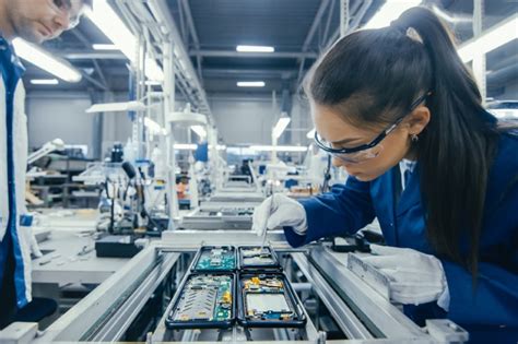
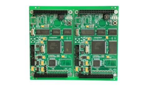
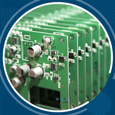
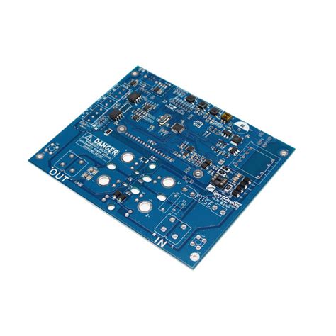
Copper clad boards, commonly referred to in the industry as PCB (Printed Circuit Boards), are essential components that form the foundation of modern electronic devices. These boards consist of a layer of copper bonded to a non-conductive substrate, providing the necessary pathways for electrical signals. The proliferation of PCB assembly (PCBA) technology has significantly advanced due to continuous innovations in manufacturing processes, allowing for increased density and functionality in electronic designs.
The evolution of copper clad boards reflects technological improvements, such as thinner copper layers and enhanced dielectric materials that lead to better performance in high-frequency applications. With the demand for smaller, more efficient devices skyrocketing, manufacturers are now focusing on reducing the weight and thickness of these circuit boards without compromising their integrity or functionality.
“The adaptability of copper clad technology is crucial as we venture further into a more connected world,” states a leading industry expert.
Contemporary challenges underscore the need for eco-friendly practices within copper clad board production. As manufacturers enhance their production techniques, they are also increasingly mindful of sustainability, utilizing materials and processes that lessen environmental impact. As a result, cutting-edge networking solutions and wearable technologies heavily depend on these advanced PCB assemblies that enhance connectivity possibilities while ensuring performance and reliability.
In summary, copper clad boards epitomize the evolution of electronics through innovation and sustainability in manufacturing practices. Their importance cannot be overstated as they not only support current technological trends but also pave the way for future advancements in electronic designs.
Technological Advancements in Copper Clad Board Manufacturing
The landscape of copper clad board manufacturing is rapidly evolving, driven by continuous technological innovations that significantly enhance the capabilities of pcb assembly and pcba processes. Manufacturers are increasingly adopting sophisticated materials and techniques that improve thermal performance and reliability, key factors in modern electronics design. One notable advancement is the integration of high-frequency laminate materials, which allow for enhanced signal integrity and reduce loss in high-speed applications. Additionally, automation in the manufacturing process has streamlined production lines, enabling rapid prototyping and customization of copper clad boards to meet specific industry needs.
Moreover, advancements in microfabrication techniques facilitate the production of intricate circuit patterns that were previously unattainable. This precision leads to better performance and compact designs—essential for the ever-shrinking real estate in electronic devices. Leading manufacturers are also investing in advanced testing methodologies to ensure quality control at every stage of production. By employing real-time monitoring systems that track environmental conditions during manufacturing, these manufacturers significantly reduce defects and waste. Such innovations not only bolster the performance characteristics of circuit boards but also promote sustainability within the industry by minimizing resource consumption.
In summary, these technological advancements play a crucial role in enhancing pcb assembly processes, allowing for more efficient pcba solutions that ultimately serve the demands of modern electronic devices while maintaining high standards for quality and environmental responsibility.
Eco-Friendly Practices Employed by Leading Manufacturers
In recent years, leading copper clad board manufacturers have made significant strides in implementing eco-friendly practices throughout the pcb assembly process. These practices not only aim to reduce the environmental impact but also contribute to the overall efficiency and sustainability of electronic products. One notable approach is the use of water-based soldering methods, which minimize hazardous emissions compared to traditional solvent-based alternatives. Additionally, manufacturers are increasingly adopting recyclable materials in their circuit boards, ensuring that the end-of-life products can be processed with minimal ecological footprint.
Another significant innovation is the commitment to energy-efficient manufacturing processes. By incorporating advanced technologies like smart materials and automation, these manufacturers can significantly reduce energy consumption during production. To further enhance their sustainability efforts, many companies are investing in renewable energy sources such as solar and wind power for their manufacturing facilities.
Here’s a brief overview of some eco-friendly practices employed by these industry leaders:
| Practice | Description |
|---|---|
| Water-Based Soldering | Reduces hazardous emissions during production |
| Use of Recyclable Materials | Minimizes ecological impact at end-of-life product disposal |
| Energy-Efficient Processes | Lowers energy consumption using advanced technologies |
| Renewable Energy Sources | Powers manufacturing facilities sustainably |
By prioritizing these sustainable methods, manufacturers are not only addressing environmental concerns but also setting a standard for future developments in the pcba industry. As a result, these eco-friendly initiatives have the potential to reshape how electronic components are produced, marking a positive shift towards more responsible manufacturing in the electronics sector. Ultimately, leading copper clad board manufacturers are paving the way for an innovative and environmentally conscious future.
Innovative Design Techniques Enhancing Circuit Board Performance
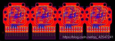
Innovative design techniques are pivotal in enhancing the performance of copper clad boards, which serve as the foundation for modern electronics. The evolution of pcb assembly processes is at the forefront of these advancements, marrying functionality with efficiency. One prominent method is the adoption of advanced simulation software that allows engineers to visualize and optimize designs before physical production. This not only reduces errors but also speeds up the pcba process, resulting in more reliable products. Additionally, techniques such as multi-layered designs and embedded components are being embraced, significantly reducing the size and weight of circuit boards while improving performance metrics. Furthermore, manufacturers are exploring novel materials and surface finishes that enhance conductivity and thermal management—crucial factors in high-performance copper clad systems. All these innovations contribute to the overall effectiveness of circuit boards, enabling them to meet the ever-increasing demands for speed and efficiency in electronic devices. As technology continues to evolve, these design strategies will play a vital role in shaping a more sustainable and advanced future for electronics.
Case Studies: Breakthrough Products from Top Manufacturers
In recent years, leading copper clad board manufacturers have introduced several innovative products that redefine the capabilities of pcba and pcb assembly processes. For instance, one notable manufacturer has developed a new type of copper clad board that incorporates high-frequency capabilities, which significantly enhances the performance of electronic devices in a wide range of applications, from telecommunications to aerospace. This advancement not only boosts signal integrity but also addresses challenges associated with traditional circuit boards.
Another manufacturer has implemented green technologies during production, resulting in eco-friendly pcb assembly methods. By using sustainable materials and adopting practices that reduce waste and energy consumption, they are paving the way for a more sustainable electronics industry. Furthermore, innovative design techniques are being utilized to create thinner and more efficient copper clad boards, which facilitate higher component density while maintaining robust electrical performance.
These case studies exemplify how top manufacturers are not merely responding to industry demands but are also anticipating future trends through continuous innovation. By focusing on cutting-edge technologies, eco-conscious practices, and design improvements, they are collectively shaping the future landscape of electronics. This shift not only enhances circuit board performance but also aligns with global efforts towards more sustainable manufacturing practices in the electronics sector.
The Future of Copper Clad Boards in the Electronics Industry
As the electronics industry continues to evolve, copper clad boards are positioned at the forefront of these advancements, playing a crucial role in enhancing performance and efficiency within various applications. The future of copper clad boards hinges on several emerging trends that promise to reshape their use in PCB assembly and PCBA processes. Manufacturers are increasingly exploring high-frequency materials and advanced layering techniques that contribute to better signal integrity, which is essential for modern electronic devices. Moreover, the integration of eco-friendly materials into production processes not only supports sustainability but also meets the rising consumer demand for greener products. Innovative designs that utilize copper clad boards, such as flexible circuits and 3D structures, are becoming prevalent as they enable more compact and versatile electronic designs. Furthermore, collaboration between leading manufacturers is fostering a competitive environment ripe for technological breakthroughs that significantly improve circuit board performance. As these trends develop, it is evident that the future of copper clad boards will be characterized by increased adaptability, enhanced functionality, and a commitment to environmental responsibility, ultimately driving further advancements in the electronics field.
Challenges and Solutions in Copper Clad Board Production
The production of copper clad boards presents several challenges that manufacturers must navigate to ensure high-quality output and efficiency. One notable challenge is the quality control of the materials used, as inconsistencies can lead to defects during the PCB assembly process. To address this, leading manufacturers have adopted rigorous testing protocols, utilizing advanced technologies for real-time monitoring during production. Additionally, environmental concerns around the use of chemicals in the manufacturing process have prompted companies to explore eco-friendly alternatives. Many copper clad board manufacturers are now integrating biodegradable materials and non-toxic processes into their workflow, significantly reducing their ecological footprint. Moreover, as the demand for high-density interconnect (HDI) designs increases in various applications, manufacturers face pressure to innovate. Implementing automation and leveraging artificial intelligence for predictive maintenance are solutions that not only enhance productivity but also improve consistency and reliability in the production of pcba components. By addressing these challenges with innovative solutions, manufacturers can enhance both performance and sustainability in the advancement of modern electronics.
Conclusion
As we explore the rapid evolution within the realm of copper clad boards, it’s evident that leading manufacturers are pushing the boundaries of innovation. The integration of advanced technologies in the pcb assembly process not only improves efficiency but also enhances the overall performance and reliability of electronic devices. The emphasis on eco-friendly practices is revolutionizing manufacturing processes, allowing for sustainable production methods that meet growing environmental concerns without sacrificing quality.
Furthermore, innovative design techniques are emerging as foundational elements in developing high-performing pcba solutions, catering to the diverse needs of the electronics industry. By employing cutting-edge materials and strategic design principles, manufacturers are able to produce circuit boards that deliver increased durability and functionality. These advancements are not merely cosmetic; they represent significant strides in meeting contemporary electronic demands.
Looking ahead, the future of copper clad boards seems poised for exciting transformations as manufacturers continue to navigate challenges while exploring opportunities for growth. As they refine production capabilities and innovate designs, we can anticipate a landscape where efficiency, sustainability, and innovation converge seamlessly, echoing a promising direction for electronics that thrives on cutting-edge solutions.
FAQs
What is a copper clad board?
A copper clad board is a crucial component in the realm of electronics, serving as the foundation for various circuit boards. This material features layers of copper laminated to a substrate, providing excellent conductivity essential for efficient pcb assembly.
How do advancements in technology impact PCB manufacturing?
Technological advancements have significantly enhanced the efficiency and performance of pcb assembly processes. Leading manufacturers are now implementing automated systems and sophisticated design software, resulting in more streamlined production and innovative pcba solutions.
What eco-friendly practices are being adopted by copper clad board manufacturers?
Many top manufacturers are prioritizing sustainability by incorporating eco-friendly materials and processes in their production lines. This includes minimizing waste, utilizing non-toxic laminating agents, and promoting recycling initiatives that not only benefit the environment but also contribute to responsible pcb assembly.
How do innovative design techniques influence circuit board performance?
Innovative design techniques play a vital role in enhancing circuit board performance. Techniques such as microvias and embedded components allow for more compact layouts and improved thermal management, maximizing functionality without increasing the size of the pcba.
What are some recent breakthroughs from leading manufacturers in this field?
Recent breakthroughs include the development of high-frequency copper clad boards that support advanced telecommunications technologies. These innovations not only improve signal integrity but also enable faster data transmission rates, which is essential for modern electronics.