Transparent PCBs: The Future of See-Through Electronics
Introduction
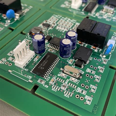
Printed Circuit Boards (PCBs) are the backbone of modern electronics, providing the necessary platform for mounting and connecting electronic components. Traditional PCBs are typically made from fiberglass (FR4) or other composite materials, which are opaque and rigid. However, with advancements in materials science and electronics manufacturing, Transparent PCBs have emerged as an innovative alternative. These see-through circuit boards combine functionality with aesthetic appeal, opening up new possibilities in consumer electronics, automotive displays, wearable technology, and more.
This article explores the technology behind transparent PCBs, their materials, manufacturing processes, applications, advantages, challenges, and future prospects.
1. What Are Transparent PCBs?
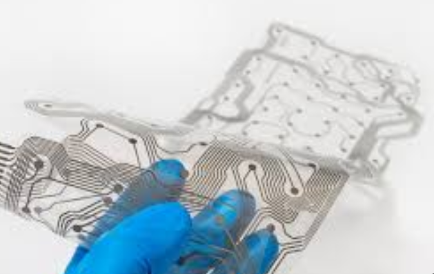
Transparent PCBs are circuit boards that allow light to pass through them while maintaining electrical conductivity. Unlike traditional PCBs, which use copper traces on an opaque substrate, transparent PCBs utilize conductive materials that are either optically clear or thin enough to maintain transparency.
Key Characteristics:
- Optical Clarity: High light transmittance (typically 70%–90%).
- Conductivity: Uses transparent conductive materials such as Indium Tin Oxide (ITO), silver nanowires, or conductive polymers.
- Flexibility: Some transparent PCBs are made on flexible substrates like PET or polyimide.
- Durability: Resistant to bending and environmental factors, depending on the material.

2. Materials Used in Transparent PCBs
The development of transparent PCBs relies on specialized materials that provide both conductivity and transparency.
A. Transparent Conductive Materials
- Indium Tin Oxide (ITO):
- Most widely used transparent conductive material.
- High conductivity and transparency (~90%).
- Brittle and expensive due to indium scarcity.
- Silver Nanowires (AgNWs):
- Flexible and highly conductive.
- Better mechanical properties than ITO.
- Used in flexible and foldable electronics.
- Conductive Polymers (PEDOT:PSS):
- Organic, flexible, and lightweight.
- Lower conductivity than ITO but improving with research.
- Graphene:
- Emerging material with excellent conductivity and transparency.
- Still in development for large-scale PCB applications.
B. Transparent Substrates
- Glass:
- Rigid and highly transparent.
- Used in displays and touch panels.
- Polyethylene Terephthalate (PET):
- Flexible and cost-effective.
- Common in wearable electronics.
- Polyimide (PI):
- High thermal stability.
- Used in high-temperature applications.

3. Manufacturing Process of Transparent PCBs
The fabrication of transparent PCBs differs from traditional PCB manufacturing due to the unique materials involved.
Key Steps:
- Substrate Preparation:
- Cleaning and treating the transparent substrate (glass/PET).
- Deposition of Conductive Layer:
- Sputtering, inkjet printing, or chemical vapor deposition (CVD) for ITO/graphene.
- Coating or printing for silver nanowires and conductive polymers.
- Patterning the Circuit:
- Photolithography or laser etching to create conductive traces.
- Component Attachment:
- Soldering or conductive adhesives for mounting components.
- Encapsulation (if flexible):
- Protective coating to prevent oxidation and mechanical damage.
4. Applications of Transparent PCBs
Transparent PCBs are finding use in multiple industries due to their unique properties.
A. Consumer Electronics
- Smartphones & Tablets:
- Used in edge-to-edge displays and under-screen circuitry.
- Wearable Devices:
- Smart glasses, transparent smartwatches.
B. Automotive Industry
- Heads-Up Displays (HUDs):
- Project information onto windshields without obstructing vision.
- Transparent Touch Panels:
- Interactive dashboards and infotainment systems.
C. Medical Devices
- See-Through Medical Sensors:
- Transparent electrodes for health monitoring.
D. Military & Aerospace
- Augmented Reality (AR) Helmets:
- Clear PCBs enable real-time data overlay.
E. Advertising & Retail
- Interactive Transparent Screens:
- Used in storefronts and digital signage.

5. Advantages of Transparent PCBs
- Aesthetic Appeal:
- Enables sleek, futuristic designs in electronics.
- Flexibility:
- Some variants can bend, enabling foldable devices.
- Lightweight:
- Ideal for portable and wearable tech.
- High Optical Clarity:
- Useful for displays and AR applications.
- Innovative Applications:
- Enables new product categories like invisible electronics.
6. Challenges & Limitations
Despite their potential, transparent PCBs face several hurdles:
- High Cost:
- ITO and silver nanowires are expensive.
- Durability Concerns:
- Some materials are prone to scratching or oxidation.
- Limited Conductivity:
- Transparent conductors have higher resistance than copper.
- Manufacturing Complexity:
- Requires specialized equipment and processes.
7. Future Trends & Developments
Research is ongoing to improve transparent PCBs:
- Alternative Materials:
- Graphene and carbon nanotubes could replace ITO.
- 3D-Printed Transparent Circuits:
- Additive manufacturing for custom designs.
- Self-Healing Conductive Layers:
- Materials that repair minor damages automatically.
- Integration with IoT & AI:
- Smart transparent surfaces with embedded sensors.

Conclusion
Transparent PCBs represent a groundbreaking shift in electronics design, merging functionality with visual elegance. While challenges remain in cost and durability, advancements in materials science and manufacturing techniques are rapidly overcoming these barriers. As industries demand more innovative and aesthetically pleasing electronic solutions, transparent PCBs are poised to play a crucial role in the future of consumer tech, automotive systems, medical devices, and beyond.
The journey toward fully transparent, high-performance electronics is just beginning, and the possibilities are as clear as the PCBs themselves.
References (if included in the original request):
- Research papers on ITO alternatives
- Industry reports on flexible electronics
- Case studies from leading electronics manufacturers
Would you like any modifications or additional details on specific sections?Introduction
Printed Circuit Boards (PCBs) are the backbone of modern electronics, providing the necessary platform for mounting and connecting electronic components. Traditional PCBs are typically made from fiberglass (FR4) or other composite materials, which are opaque and rigid. However, with advancements in materials science and electronics manufacturing, Transparent PCBs have emerged as an innovative alternative. These see-through circuit boards combine functionality with aesthetic appeal, opening up new possibilities in consumer electronics, automotive displays, wearable technology, and more.
This article explores the technology behind transparent PCBs, their materials, manufacturing processes, applications, advantages, challenges, and future prospects.


