Uncovering the secrets of PCB manufacturing process
Before the emergence of PCB, circuits were made up of point-to-point wiring. This method has low reliability because as the circuit ages, the rupture of the line will cause the circuit node to be broken or short-circuited. Winding technology is a major advancement in circuit technology. This method improves the durability and replaceability of the circuit by winding small-diameter wire around the pillars of the connection point.
As the electronics industry developed from vacuum tubes and relays to silicon semiconductors and integrated circuits, the size and price of electronic components also decreased. Electronic products are appearing more and more frequently in the consumer field, prompting manufacturers to find smaller and more cost-effective solutions. Thus, PCB was born.
PCB manufacturing process
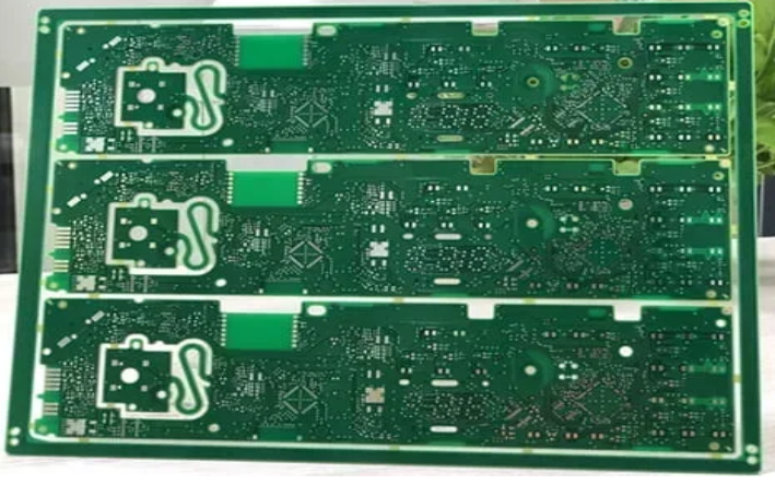
The production of PCB is very complicated. Taking a four-layer printed circuit board as an example, its production process mainly includes PCB layout, core board production, inner PCB layout transfer, core board punching and inspection, lamination, drilling, copper chemical precipitation of hole wall, outer PCB layout transfer, outer PCB etching and other steps.
1.PCB layout
The first step in PCB production is to organize and check the PCB layout (Layout). The PCB manufacturing factory receives the CAD file from the PCB design company. Since each CAD software has its own unique file format, the PCB factory will convert it into a unified format – Extended Gerber RS-274X or Gerber X2. Then the factory engineer will check whether the PCB layout meets the manufacturing process and whether there are any defects. 2. Production of the core board Clean the copper clad board. If there is dust, it may cause the final circuit to short or open.
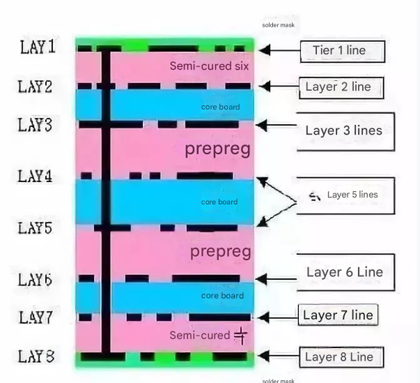
The figure below is an example of an 8-layer PCB. In fact, it is composed of 3 copper clad boards (core boards) plus 2 copper films, which are then glued together with prepreg. The production sequence starts from the middle core board (4th and 5th layer circuits), and then continuously stacked together and fixed. The production of 4-layer PCB is similar, except that only 1 core board and 2 copper films are used.

3.The transfer of the inner layer PCB layout must first make the two layers of circuits of the middle core board (Core). After the copper clad laminate is cleaned, a layer of photosensitive film will be covered on the surface. This film will solidify when exposed to light, forming a protective film on the copper foil of the copper clad laminate.
Insert the two-layer PCB layout film and the double-layer copper clad laminate, and finally insert the upper PCB layout film to ensure the accurate stacking position of the upper and lower PCB layout films.
The photosensitive machine uses a UV lamp to irradiate the photosensitive film on the copper foil. Under the light-transmitting film, the photosensitive film is solidified, and under the opaque film, there is still no solidified photosensitive film. The copper foil covered under the solidified photosensitive film is the required PCB layout circuit, which is equivalent to the role of laser printer ink for manual PCB. Then use alkali to clean the unsolidified photosensitive film, and the required copper foil circuit will be covered by the solidified photosensitive film.
Then use a strong alkali, such as NaOH, to etch away the unnecessary copper foil.
Tear off the solidified photosensitive film to expose the required PCB layout circuit copper foil.
4.Core board punching and inspection
The core board has been successfully manufactured. Then make alignment holes on the core board to facilitate alignment with other raw materials. Once the core board is pressed together with other layers of PCB, it cannot be modified, so inspection is very important. The machine will automatically compare it with the PCB layout drawing to check for errors.
5.Lamination
Here a new raw material called prepreg is needed, which is the adhesive between the core board and the core board (PCB layer number>4), and between the core board and the outer copper foil, and also plays an insulating role. The lower copper foil and two layers of prepreg have been fixed in place in advance through the alignment holes and the lower iron plate, and then the prepared core board is also placed in the alignment holes, and finally two layers of prepreg, a layer of copper foil and a layer of pressure-bearing aluminum plate are covered on the core board in turn.
The PCB boards clamped by the iron plate are placed on the bracket and then sent to the vacuum hot press for lamination. The high temperature in the vacuum hot press can melt the epoxy resin in the prepreg and fix the core boards and copper foils together under pressure.
After lamination, remove the upper iron plate that presses the PCB. Then take away the pressure-bearing aluminum plate, which also serves to isolate different PCBs and ensure the smoothness of the outer copper foil of the PCB. At this time, both sides of the PCB taken out will be covered with a layer of smooth copper foil.
6. Drilling
To connect the 4 layers of copper foil in the PCB that are not in contact, first drill through holes from top to bottom to open the PCB, and then metalize the hole wall to conduct electricity. Use an X-ray drilling machine to locate the inner core board. The machine will automatically find and locate the hole position on the core board, and then punch a positioning hole in the PCB to ensure that the next drilling is through the center of the hole position.
Place a layer of aluminum plate on the punching machine, and then place the PCB on it. In order to improve efficiency, 1 to 3 identical PCB boards will be stacked together for perforation according to the number of layers of the PCB. Finally, cover the top PCB with a layer of aluminum plate. The upper and lower layers of aluminum plates are to prevent the copper foil on the PCB from being torn when the drill drills in and out.
In the previous lamination process, the melted epoxy resin was squeezed out of the PCB, so it needs to be cut off. The template milling machine cuts the periphery of the PCB according to the correct XY coordinates of the PCB.
7.Chemical deposition of copper on the hole wall
Since almost all PCB designs use perforations to connect different layers of circuits, a good connection requires a 25-micron copper film on the hole wall. This thickness of copper film needs to be achieved through electroplating, but the hole wall is composed of non-conductive epoxy resin and fiberglass board. So the first step is to accumulate a layer of conductive material on the hole wall, and form a 1-micron copper film on the entire PCB surface, including the hole wall, by chemical deposition. The whole process, such as chemical treatment and cleaning, is controlled by the machine.
Fixing PCB
Cleaning PCB
Transporting PCB8. Transfer of outer PCB layout Next, the outer PCB layout will be transferred to the copper foil. The process is similar to the previous inner core board PCB layout transfer principle. Both use photocopied film and photosensitive film to transfer the PCB layout to the copper foil. The only difference is that the positive film will be used to make the board. The inner PCB layout transfer uses the subtractive method, and the negative film is used to make the board. The circuits are covered by the cured photosensitive film on the PCB. After the uncured photosensitive film is cleaned and the exposed copper foil is etched, the PCB layout circuits are protected by the cured photosensitive film and remain. The outer PCB layout transfer adopts the normal method, using positive film as the board. The non-circuit area is covered by the cured photosensitive film on the PCB. After cleaning the uncured photosensitive film, electroplating is performed. The film cannot be electroplated, and the copper is first plated and then tin is plated in the absence of the film. After the film is removed, alkaline etching is performed, and finally the tin is removed. The circuit pattern remains on the board because it is protected by tin.
Clamp the PCB with a clamp and electroplate the copper. As mentioned earlier, in order to ensure that the hole position has good enough conductivity, the copper film electroplated on the hole wall must have a thickness of 25 microns, so the entire system will be automatically controlled by a computer to ensure its accuracy. 9. Etching of the outer PCB Next, a complete automated assembly line completes the etching process. First, the cured photosensitive film on the PCB board is cleaned. Then use strong alkali to clean off the unnecessary copper foil covered by it. Then use tin stripping liquid to remove the tin plating on the copper foil of the PCB layout. After cleaning, the 4-layer PCB layout is completed.