Understanding 8-Layer PCBs: Design, Applications, and Manufacturing Considerations
In the world of modern electronics, the demand for high-performance, compact, and multifunctional devices has driven the need for complex printed circuit boards (PCBs). Among the various types of PCBs, 8-layer PCBs have emerged as a popular choice for advanced applications that require high density, signal integrity, and thermal management. This article provides a comprehensive overview of 8-layer PCBs, including their structure, design considerations, applications, and manufacturing challenges.
What Is an 8-Layer PCB?
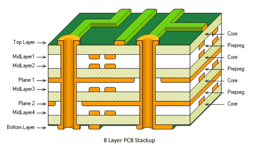
An 8-layer PCB is a multilayer printed circuit board consisting of eight conductive copper layers separated by insulating dielectric materials. These layers are interconnected through vias, which allow electrical signals to travel between layers. The stack-up of an 8-layer PCB typically includes signal layers, power planes, and ground planes, arranged in a specific configuration to optimize performance.
Structure of an 8-Layer PCB
The layer stack-up of an 8-layer PCB is carefully designed to meet the electrical, thermal, and mechanical requirements of the application. A typical 8-layer stack-up might look like this:
- Top Layer (Signal Layer): Used for component placement and high-speed signal routing.
- Ground Plane: Provides a low-impedance return path for signals and reduces electromagnetic interference (EMI).
- Signal Layer: Routes high-speed or sensitive signals.
- Power Plane: Distributes power to components and reduces voltage drop.
- Signal Layer: Routes additional signals, often with controlled impedance.
- Ground Plane: Enhances EMI shielding and signal integrity.
- Signal Layer: Routes low-speed or less critical signals.
- Bottom Layer (Signal Layer): Used for component placement and additional signal routing.
This stack-up can be customized based on the specific requirements of the design, such as the need for additional power planes or signal layers.
Advantages of 8-Layer PCBs
8-layer PCBs offer several advantages over simpler PCBs, such as 2-layer or 4-layer designs:
- High Density: The additional layers allow for more complex routing and higher component density, making 8-layer PCBs ideal for compact devices.
- Improved Signal Integrity: Dedicated ground and power planes reduce noise and crosstalk, ensuring clean signal transmission.
- Better Thermal Management: The multiple layers provide more pathways for heat dissipation, improving thermal performance.
- Enhanced EMI Shielding: Ground planes between signal layers minimize electromagnetic interference, making 8-layer PCBs suitable for high-frequency applications.
- Design Flexibility: The extra layers enable designers to route high-speed signals, power, and ground more efficiently, reducing design constraints.
Applications of 8-Layer PCBs
8-layer PCBs are used in a wide range of advanced applications across various industries. Some of the most common applications include:
- Telecommunications:
- 8-layer PCBs are widely used in networking equipment, routers, and switches, where high-speed signal integrity and EMI shielding are critical.
- Consumer Electronics:
- Smartphones, tablets, and laptops often use 8-layer PCBs to accommodate high-density components and high-speed interfaces like USB-C and HDMI.
- Aerospace and Defense:
- Avionics, radar systems, and satellite communication equipment rely on 8-layer PCBs for their reliability and performance in harsh environments.
- Medical Devices:
- Advanced medical equipment, such as MRI machines and patient monitoring systems, use 8-layer PCBs to ensure precision and reliability.
- Automotive Electronics:
- Modern vehicles incorporate 8-layer PCBs in engine control units (ECUs), infotainment systems, and advanced driver-assistance systems (ADAS).
- Industrial Automation:
- High-performance industrial controllers and robotics often use 8-layer PCBs to handle complex signal routing and power distribution.

Design Considerations for 8-Layer PCBs
Designing an 8-layer PCB requires careful planning and attention to detail to ensure optimal performance and manufacturability. Here are some key considerations:
1. Layer Stack-Up
- Choose a stack-up configuration that balances signal integrity, power distribution, and thermal management. Common configurations include:
- Signal-Ground-Signal-Power-Signal-Ground-Signal-Signal
- Signal-Ground-Signal-Power-Ground-Signal-Ground-Signal
2. Signal Integrity
- Use controlled impedance routing for high-speed signals to minimize reflections and crosstalk.
- Place ground planes adjacent to signal layers to provide a low-impedance return path.
3. Power Integrity
- Distribute power planes evenly to reduce voltage drop and ensure stable power delivery.
- Use decoupling capacitors near high-power components to suppress noise.
4. Thermal Management
- Incorporate thermal vias to transfer heat from high-power components to inner layers or heat sinks.
- Use copper pours on outer layers to improve heat dissipation.
5. EMI and EMC
- Follow best practices for EMI shielding, such as placing ground planes between signal layers and avoiding split planes.
- Use proper grounding techniques to minimize electromagnetic compatibility (EMC) issues.
6. Component Placement
- Place high-speed components close to their respective signal layers to minimize trace lengths and signal degradation.
- Group related components together to simplify routing and reduce noise.
7. Manufacturability
- Adhere to the manufacturer’s design rules, including minimum trace width, spacing, and via size.
- Use standard materials and processes to reduce costs and lead times.
Manufacturing Challenges for 8-Layer PCBs
The manufacturing process for 8-layer PCBs is more complex than that of simpler PCBs, presenting several challenges:
- Alignment and Registration:
- Ensuring precise alignment of all eight layers during lamination is critical to avoid misregistration and signal integrity issues.
- Drilling and Plating:
- Drilling and plating vias in an 8-layer PCB require high precision to ensure reliable electrical connections between layers.
- Material Selection:
- Choosing the right dielectric materials and copper weights is essential for achieving the desired electrical and thermal performance.
- Quality Control:
- Rigorous testing and inspection are required to detect defects such as delamination, voids, or shorts.
- Cost and Lead Time:
- The complexity of 8-layer PCBs increases manufacturing costs and lead times compared to simpler designs.
Best Practices for Designing 8-Layer PCB
To overcome these challenges and ensure a successful design, follow these best practices:
- Collaborate with Your Manufacturer:
- Work closely with your PCB manufacturer to understand their capabilities and design rules.
- Use Simulation Tools:
- Leverage signal integrity and thermal simulation tools to validate your design before fabrication.
- Optimize Layer Stack-Up:
- Choose a stack-up configuration that meets your electrical and thermal requirements while minimizing complexity.
- Follow Design Guidelines:
- Adhere to industry standards and best practices for trace routing, via placement, and component spacing.
- Prototype and Test:
- Build and test prototypes to identify and address any issues before moving to full production.
Conclusion
8-layer PCBs are a powerful solution for advanced electronics applications that require high density, signal integrity, and thermal management. By understanding the structure, design considerations, and manufacturing challenges of 8-layer PCBs, engineers can create reliable and high-performance designs that meet the demands of modern technology.
As the electronics industry continues to evolve, the importance of 8-layer PCBs will only grow, enabling innovations in telecommunications, consumer electronics, aerospace, and beyond. By leveraging best practices and collaborating with experienced manufacturers, designers can unlock the full potential of 8-layer PCBs and push the boundaries of what is possible in electronics design.


