Understanding ADC Basic Parameters and Strategies to Improve ADC Performance
Introduction
Analog-to-Digital Converters (ADCs) are critical components in modern electronic systems, converting continuous analog signals into discrete digital values for processing by digital systems. The performance of an ADC significantly impacts the accuracy and reliability of data acquisition systems, communication devices, medical instruments, and industrial control systems. To optimize ADC performance, engineers must understand key ADC parameters and implement strategies to enhance their operation. This article explores the fundamental parameters of ADCs and discusses techniques to improve their performance.
1. Basic ADC Parameters
The performance of an ADC is characterized by several key parameters. Understanding these parameters is essential for selecting the right ADC for a given application and optimizing its performance.
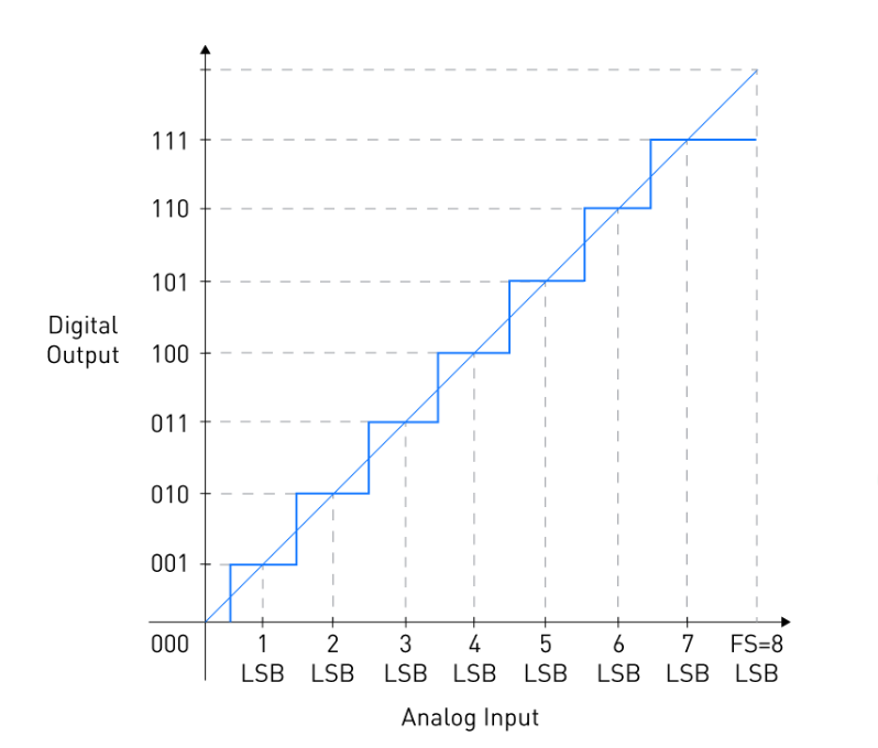
1.1 Resolution
- Definition: Resolution refers to the number of discrete digital levels an ADC can produce to represent an analog signal. It is typically expressed in bits (e.g., 8-bit, 12-bit, 16-bit).
- Impact: Higher resolution allows finer signal representation but increases complexity and conversion time.
- Example: A 12-bit ADC can represent an analog signal with 4096 (2¹²) discrete levels.
1.2 Sampling Rate (Fs)
- Definition: The sampling rate is the number of samples an ADC can convert per second, measured in samples per second (SPS) or Hertz (Hz).
- Impact: A higher sampling rate allows capturing faster signal variations but requires more processing power.
- Nyquist Theorem: The sampling rate must be at least twice the highest frequency component of the input signal (Nyquist rate) to avoid aliasing.
1.3 Signal-to-Noise Ratio (SNR)
- Definition: SNR measures the ratio of the desired signal power to the noise power, expressed in decibels (dB).
- Impact: A higher SNR indicates better signal clarity and less distortion.
- Calculation:
[
SNR = 6.02 \times N + 1.76 \, \text{dB} \quad (\text{where } N = \text{number of bits})
]
1.4 Effective Number of Bits (ENOB)
- Definition: ENOB indicates the actual resolution of an ADC after accounting for noise and distortion.
- Impact: Real-world ADCs rarely achieve their theoretical SNR due to noise; ENOB provides a more practical measure of performance.
- Formula:
[
ENOB = \frac{SNR – 1.76}{6.02}
]
1.5 Total Harmonic Distortion (THD)
- Definition: THD measures the distortion introduced by harmonics of the input signal, expressed as a percentage or in dB.
- Impact: Lower THD means better signal fidelity.
- Calculation:
[
THD = \sqrt{\frac{V_2^2 + V_3^2 + \dots + V_n^2}{V_1^2}} \times 100\%
]
(where (V_1) is the fundamental frequency and (V_2, V_3, \dots) are harmonics)
1.6 Integral Non-Linearity (INL)
- Definition: INL measures the deviation of an ADC’s transfer function from a straight line, typically expressed in least significant bits (LSBs).
- Impact: High INL introduces non-linear errors, degrading accuracy.
1.7 Differential Non-Linearity (DNL)
- Definition: DNL measures the difference between actual and ideal step widths in an ADC’s output.
- Impact: Poor DNL can cause missing codes or non-monotonic behavior.
1.8 Power Consumption
- Definition: The amount of power an ADC consumes during operation.
- Impact: High-speed, high-resolution ADCs typically consume more power, affecting battery life and thermal management.
1.9 Input Voltage Range
- Definition: The range of analog input voltages that an ADC can convert.
- Impact: Must match the signal range to avoid clipping or underutilization.
1.10 Conversion Latency
- Definition: The time delay between the start of conversion and the availability of the digital output.
- Impact: Critical in real-time applications like control systems and high-speed data acquisition.
2. Techniques to Improve ADC Performance
To maximize ADC performance, engineers must optimize both the ADC selection and the surrounding circuitry. Below are key strategies to enhance ADC performance.
2.1 Optimizing the Front-End Circuitry
- Anti-Aliasing Filter (AAF):
- A low-pass filter should be used to remove high-frequency noise above the Nyquist frequency.
- Prevents aliasing and improves signal integrity.
- Proper Signal Conditioning:
- Amplify weak signals using low-noise amplifiers (LNAs).
- Use impedance matching to minimize signal reflections.
2.2 Reducing Noise and Interference
- Grounding and Shielding:
- Use a solid ground plane to minimize ground loops.
- Shield sensitive analog traces from digital noise.
- Decoupling Capacitors:
- Place bypass capacitors near the ADC’s power pins to filter high-frequency noise.
- Twisted-Pair or Differential Signaling:
- Reduces electromagnetic interference (EMI) in high-noise environments.
2.3 Improving Clock Stability
- Low-Jitter Clock Source:
- Clock jitter introduces timing errors, degrading SNR.
- Use crystal oscillators or phase-locked loops (PLLs) for stable clocking.
- Synchronous Sampling:
- Ensures consistent sampling intervals, reducing timing errors.
2.4 Calibration Techniques
- Offset and Gain Calibration:
- Corrects DC offset and gain errors using software or hardware adjustments.
- Background Calibration:
- Continuously calibrates the ADC during operation to compensate for temperature drift.
2.5 Using Oversampling and Averaging
- Oversampling:
- Sampling at a rate higher than Nyquist improves resolution by spreading noise over a wider bandwidth.
- Digital Averaging:
- Reduces random noise by averaging multiple samples.
2.6 Choosing the Right ADC Architecture
Different ADC architectures (e.g., SAR, Delta-Sigma, Pipeline, Flash) have trade-offs in speed, resolution, and power consumption:
- Successive Approximation Register (SAR) ADC:
- Good for medium-speed, medium-resolution applications.
- Delta-Sigma (ΔΣ) ADC:
- High resolution but slower, ideal for precision measurements.
- Pipeline ADC:
- High-speed, moderate resolution, used in communication systems.
- Flash ADC:
- Extremely fast but lower resolution and high power consumption.
2.7 Managing Power Supply Noise
- Separate Analog and Digital Supplies:
- Prevents digital switching noise from coupling into the analog section.
- Low-Dropout Regulators (LDOs):
- Provide clean power to sensitive ADC components.
2.8 Thermal Management
- Temperature Compensation:
- Some ADCs include built-in temperature sensors for drift correction.
- Heat Sinking:
- High-speed ADCs may require cooling to maintain performance.
3. Conclusion
ADCs are vital in bridging the analog and digital worlds, and their performance directly affects system accuracy and reliability. By understanding key ADC parameters—such as resolution, sampling rate, SNR, ENOB, and non-linearity—engineers can make informed design choices. Furthermore, optimizing front-end circuitry, reducing noise, improving clock stability, and employing calibration techniques can significantly enhance ADC performance. Selecting the appropriate ADC architecture and managing power and thermal issues further ensure optimal operation in demanding applications.
As technology advances, ADCs continue to evolve, offering higher speeds, better resolution, and lower power consumption. By applying the principles discussed in this article, engineers can maximize ADC performance and deliver robust, high-precision electronic systems.