Understanding Electrical Clearance, Creepage Distance, and the Purpose of Slotting in PCBs
Introduction
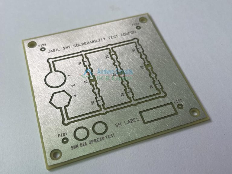
Printed Circuit Boards (PCBs) are fundamental components in modern electronics, providing mechanical support and electrical connections for various components. To ensure safety, reliability, and compliance with industry standards, PCB designers must consider several critical factors, including electrical clearance, creepage distance, and the need for slotting (or milling) on PCBs. This article explores these concepts in detail, explaining their definitions, importance, and practical applications in PCB design.
1. Electrical Clearance
Definition
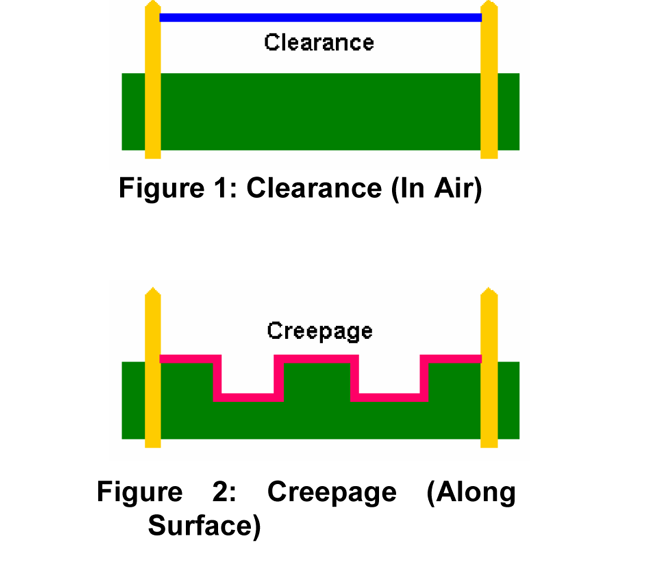
Electrical clearance refers to the shortest distance through air between two conductive parts (e.g., traces, pads, or components) on a PCB. It is the minimum separation required to prevent electrical arcing or breakdown due to high voltage differences.
Factors Affecting Electrical Clearance
Several factors influence the required electrical clearance:
- Voltage Level: Higher voltages require larger clearances to prevent arcing.
- Environmental Conditions: Humidity, pollution, and altitude affect air insulation properties.
- PCB Material: The dielectric strength of the PCB substrate impacts clearance requirements.
- Regulatory Standards: Standards like IPC-2221, IEC 60950, and UL 61010 define minimum clearance values.
Why is Electrical Clearance Important?
- Prevents Short Circuits: Ensures conductors do not unintentionally discharge.
- Avoids Arcing: High-voltage differences can ionize air, leading to sparks.
- Compliance with Safety Standards: Ensures the PCB meets industry regulations.
Example Calculation
According to IPC-2221, for an internal conductor (uncoated) at 100V DC in a normal environment, the minimum clearance is 0.1 mm. For 1000V, it increases to 2.5 mm.
2. Creepage Distance
Definition
Creepage distance is the shortest path along the surface of an insulating material between two conductive parts. Unlike clearance (which is through air), creepage considers surface contamination, moisture, and dust that can create conductive paths.
Factors Affecting Creepage Distance
- Pollution Degree: Dusty or humid environments require larger creepage distances.
- Material CTI (Comparative Tracking Index): Measures a material’s resistance to surface tracking (higher CTI = better insulation).
- Voltage and Frequency: Higher voltages and AC signals increase tracking risk.
Why is Creepage Distance Important?
- Prevents Surface Tracking: Avoids leakage currents due to contamination.
- Enhances Long-Term Reliability: Reduces risk of degradation over time.
- Compliance with Safety Standards: Standards like IEC 60664 specify minimum creepage distances.
Example Calculation
For a 250V AC circuit in a Pollution Degree 2 environment with a CTI ≥ 175, the minimum creepage distance is 2.5 mm (per IEC 60664).
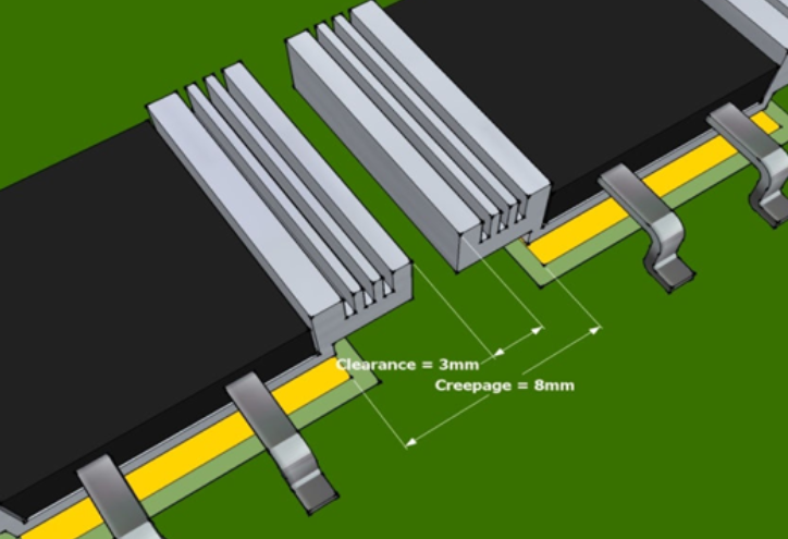
3. Why Do PCBs Need Slotting (Cutouts)?
Definition
Slotting (or milling) refers to creating non-conductive cutouts or openings in a PCB. These can be used for mechanical, thermal, or electrical isolation purposes.
Reasons for Slotting in PCBs
- High-Voltage Isolation
- Slots increase creepage distance between high-voltage traces by forcing current to travel around the gap.
- Example: In power supplies, slots separate primary (high-voltage) and secondary (low-voltage) sides.
- Preventing Arc Formation
- In high-voltage PCBs, slots prevent arcing between adjacent conductors.
- Thermal Management
- Slots help dissipate heat by increasing airflow or separating heat-sensitive components.
- Mechanical Stability
- Reduces stress on the PCB, preventing warping or cracking.
- Used in flexible PCBs to allow bending.
- EMI Reduction
- Slots can act as barriers to electromagnetic interference (EMI) by breaking ground plane loops.
- Assembly and Mounting
- Slots allow screws or connectors to be mounted securely.
Common Applications of PCB Slotting
- Isolation in Power Electronics (e.g., AC/DC converters)
- High-Frequency Circuits (RF/microwave PCBs)
- Industrial and Automotive PCBs (high-reliability applications)
4. Design Considerations for Clearance, Creepage, and Slotting
Best Practices for PCB Layout
- Follow Industry Standards (IPC, IEC, UL)
- Use High-CTI Materials for better insulation.
- Increase Creepage with Slots when needed.
- Avoid Sharp Edges (round corners reduce discharge risk).
- Conformal Coating can enhance insulation in harsh environments.
Software Tools for Verification
- Altium Designer, KiCad, and Cadence include DRC (Design Rule Check) tools to validate clearance and creepage.
- Simulation Tools (e.g., ANSYS) can predict arcing risks.
5. Conclusion
Understanding electrical clearance, creepage distance, and PCB slotting is essential for designing safe and reliable circuit boards. These factors prevent electrical failures, ensure compliance with safety standards, and improve PCB performance in demanding environments. By following best practices and leveraging modern design tools, engineers can optimize PCB layouts for high-voltage, high-frequency, and industrial applications.