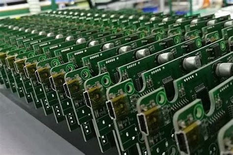
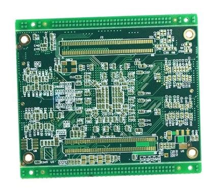
Understanding Filter PCBs: Design, Applications, and Best Practices
In the realm of electronics, filters play a crucial role in shaping and controlling signals. Whether it’s removing noise from a power supply, isolating specific frequencies in a communication system, or ensuring signal integrity in high-speed circuits, filters are indispensable. Filter PCBs, or printed circuit boards specifically designed to incorporate filtering functions, are at the heart of many modern electronic systems. This article delves into the design principles, applications, and best practices for filter PCBs, providing a comprehensive guide for engineers and designers.
What Are Filter PCBs?
Filter PCBs are specialized printed circuit boards that integrate filtering components and circuits to achieve specific signal processing tasks. These PCBs are designed to pass desired frequencies while attenuating unwanted ones, ensuring clean and reliable signal transmission. Filters can be categorized into several types based on their frequency response:
- Low-Pass Filters (LPF): Allow low-frequency signals to pass while attenuating high-frequency signals.
- High-Pass Filters (HPF): Allow high-frequency signals to pass while attenuating low-frequency signals.
- Band-Pass Filters (BPF): Allow a specific range of frequencies to pass while attenuating frequencies outside this range.
- Band-Stop Filters (BSF): Attenuate a specific range of frequencies while allowing others to pass.
- Notch Filters: A type of band-stop filter that targets a very narrow range of frequencies.
Filter PCBs can be implemented using various technologies, including passive components (resistors, capacitors, and inductors), active components (op-amps and transistors), and even advanced materials like ceramic or SAW (Surface Acoustic Wave) filters.
Key Components of Filter PCBs
The design of a filter PCB involves several key components and considerations:
1. Passive Components
- Resistors (R): Used to control signal amplitude and impedance matching.
- Capacitors (C): Store and release electrical energy, crucial for frequency-dependent behavior.
- Inductors (L): Store energy in a magnetic field, essential for filtering and impedance matching.
2. Active Components
- Operational Amplifiers (Op-Amps): Used in active filter designs to provide gain and improve performance.
- Transistors: Used in more complex filter designs, such as switched-capacitor filters.
3. Substrate Material
- The choice of PCB material affects the performance of the filter. High-frequency applications may require specialized materials like Rogers laminates, which offer low dielectric loss and stable performance.
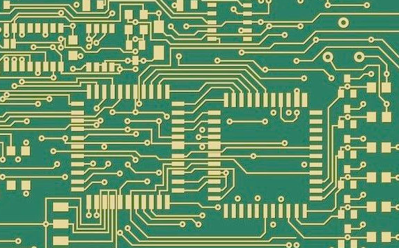
4. Trace Geometry
- The layout of traces on the PCB can influence the filter’s performance. Proper impedance matching and minimizing parasitic capacitance and inductance are critical.
5. Grounding and Shielding
- Effective grounding and shielding techniques are essential to minimize noise and interference, ensuring the filter operates as intended.
Design Considerations for Filter PCBs
Designing a filter PCB requires careful consideration of several factors to achieve the desired performance. Here are some key design considerations:
1. Filter Type and Specifications
- Determine the type of filter (LPF, HPF, BPF, BSF) and its specifications, such as cutoff frequency, passband ripple, and stopband attenuation.
- Use filter design tools and software to simulate and optimize the filter’s response.
2. Component Selection
- Choose components with appropriate values and tolerances to meet the filter’s specifications.
- Consider the temperature coefficient and stability of components, especially for high-precision applications.
3. PCB Layout
- Minimize trace lengths to reduce parasitic inductance and capacitance.
- Use ground planes and proper decoupling capacitors to reduce noise and improve signal integrity.
- Ensure proper spacing between components to avoid crosstalk and interference.
4. Impedance Matching
- Match the impedance of the filter to the source and load to minimize reflections and signal loss.
- Use transmission line techniques for high-frequency applications.
5. Thermal Management
- Consider the power dissipation of components and ensure adequate thermal management to prevent overheating.
- Use thermal vias and heat sinks if necessary.
6. Testing and Validation
- Perform thorough testing and validation to ensure the filter meets its specifications.
- Use network analyzers and spectrum analyzers to measure the filter’s frequency response and performance.
Applications of Filter PCBs
Filter PCBs are used in a wide range of applications across various industries. Here are some notable examples:
1. Telecommunications
- RF Filters: Used in wireless communication systems to isolate specific frequency bands and reduce interference.
- Baseband Filters: Used in modems and transceivers to shape and process baseband signals.
2. Audio Equipment
- Crossover Networks: Used in speakers to separate audio signals into different frequency bands for drivers (woofers, tweeters).
- Noise Reduction: Used in audio processing equipment to remove noise and enhance signal quality.
3. Power Supplies
- EMI Filters: Used to suppress electromagnetic interference in power supplies and ensure compliance with regulatory standards.
- DC-DC Converters: Used to filter output voltage and reduce ripple.
4. Medical Devices
- Signal Processing: Used in medical imaging and diagnostic equipment to process and filter signals from sensors and transducers.
- Noise Reduction: Used in patient monitoring systems to remove noise and artifacts from physiological signals.
5. Automotive Electronics
- Engine Control Units (ECUs): Used to filter sensor signals and ensure accurate control of engine parameters.
- Infotainment Systems: Used to process audio and video signals and reduce interference.
6. Aerospace and Defense
- Radar Systems: Used to filter and process radar signals for target detection and tracking.
- Communication Systems: Used to filter and isolate communication channels in avionics and satellite systems.
Best Practices for Designing Filter PCBs
To ensure optimal performance and reliability, follow these best practices when designing filter PCBs:
1. Start with a Clear Specification
- Define the filter’s requirements, including frequency range, attenuation, and passband ripple.
- Use simulation tools to model the filter’s response and optimize its design.
2. Choose the Right Components
- Select components with appropriate values, tolerances, and temperature coefficients.
- Consider using surface-mount devices (SMDs) for compact and high-performance designs.
3. Optimize the PCB Layout
- Minimize trace lengths and avoid sharp corners to reduce parasitic effects.
- Use ground planes and proper decoupling to minimize noise and interference.
4. Ensure Proper Impedance Matching
- Match the impedance of the filter to the source and load to minimize reflections and signal loss.
- Use transmission line techniques for high-frequency applications.
5. Implement Effective Thermal Management
- Consider the power dissipation of components and ensure adequate thermal management.
- Use thermal vias and heat sinks if necessary.
6. Test and Validate the Design
- Perform thorough testing and validation to ensure the filter meets its specifications.
- Use network analyzers and spectrum analyzers to measure the filter’s frequency response and performance.
7. Consider Environmental Factors
- Design for the operating environment, including temperature, humidity, and vibration.
- Use conformal coatings or encapsulation to protect the PCB from environmental damage.
Challenges and Solutions in Filter PCB Design
Designing filter PCBs presents several challenges, but these can be addressed with the right strategies:
- Parasitic Effects:
- Challenge: Parasitic capacitance and inductance can alter the filter’s response.
- Solution: Minimize trace lengths and use proper layout techniques to reduce parasitic effects.
- Component Tolerance:
- Challenge: Variations in component values can affect the filter’s performance.
- Solution: Use components with tight tolerances and perform thorough testing to ensure consistency.
- Thermal Management:
- Challenge: High-power components can generate heat, affecting the filter’s performance.
- Solution: Implement effective thermal management techniques, such as thermal vias and heat sinks.
- Signal Integrity:
- Challenge: Noise and interference can degrade the filter’s performance.
- Solution: Use proper grounding, shielding, and decoupling techniques to maintain signal integrity.
- Cost and Complexity:
- Challenge: High-performance filters can be complex and costly to design and manufacture.
- Solution: Balance performance and cost by optimizing the design and selecting cost-effective components.
Conclusion
Filter PCBs are essential components in modern electronic systems, enabling precise signal processing and noise reduction across a wide range of applications. By understanding the design principles, applications, and best practices for filter PCBs, engineers and designers can create high-performance, reliable filters that meet the demands of their specific use cases.
As technology continues to advance, the importance of filter PCBs will only grow, particularly in fields such as telecommunications, medical devices, and automotive electronics. By leveraging advanced design tools, simulation techniques, and high-quality materials, designers can push the boundaries of what is possible with filter PCBs, enabling innovative solutions for the electronics of tomorrow.


