Understanding First-Order and Second-Order PCB in HDI Manufacturing Processes
Introduction to HDI PCB Technology
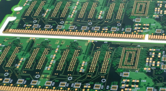
High Density Interconnect (HDI) printed circuit boards represent the cutting edge of PCB technology, enabling the production of smaller, faster, and more complex electronic devices. As consumer electronics continue to demand more functionality in increasingly compact form factors, HDI technology has become essential for modern PCB manufacturing. At the heart of HDI manufacturing lies the concept of different “orders” of PCBs—particularly first-order and second-order boards—which define their complexity and manufacturing processes.
This article will explore in detail what distinguishes first-order from second-order HDI PCBs, their manufacturing processes, design considerations, and applications in today’s electronics industry. Understanding these classifications is crucial for engineers, designers, and procurement specialists working with advanced PCB technologies.
Fundamentals of HDI PCB Technology
What Makes a PCB “HDI”?
HDI PCBs differ from conventional printed circuit boards in several key aspects:
- Higher wiring density: HDI boards pack more circuitry into less space
- Finer lines and spaces: Typically below 100μm (4 mil)
- Smaller vias: Including microvias (usually <150μm in diameter)
- Thinner materials: Enabling more compact designs
- Sequential lamination: Multiple lamination cycles for complex interconnects
The transition from conventional PCBs to HDI technology has been driven by the need for:
- Miniaturization of electronic devices
- Increased functionality in smaller packages
- Improved signal integrity at higher frequencies
- Enhanced thermal management
- Reduced weight in portable electronics
The Order Classification System
The “order” of an HDI PCB refers to the complexity of its microvia interconnect structure. This classification helps manufacturers and designers communicate about the board’s capabilities and manufacturing requirements. The order system primarily describes:
- How many times the board undergoes lamination cycles
- The arrangement and stacking of microvias
- The complexity of the interconnect architecture
While there are higher-order HDI PCBs (third-order and beyond), first-order and second-order boards represent the most commonly used configurations in the industry today.
First-Order HDI PCBs
Definition and Characteristics
First-order HDI PCBs represent the entry point into high-density interconnect technology. These boards feature:
- Single lamination cycle after the core fabrication
- 1+N+1 layer structure (where N is the number of core layers)
- Non-stacked microvias that don’t align vertically between layers
- Simplest HDI architecture while still offering significant space savings
A typical first-order HDI stackup might look like:
- Top layer (with components)
- Microvia layer
- Core layers (traditional through-hole vias)
- Microvia layer
- Bottom layer (with components)
Manufacturing Process
The production of first-order HDI PCBs follows these key steps:
- Core fabrication: Manufacturing the conventional multilayer core using standard PCB processes
- Laser drilling: Creating microvias in the dielectric layers above and below the core
- Plating: Metallizing the microvias to establish electrical connections
- Patterning: Creating the fine-line circuitry on the outer layers
- Lamination: Bonding all layers together in a single pressing operation
- Final processing: Including solder mask application, surface finishing, and testing
Design Considerations
When designing first-order HDI PCBs, engineers must consider:
- Microvia placement: Non-stacked arrangement requires careful routing planning
- Signal integrity: Proper management of high-speed signals transitioning between microvias and through-hole vias
- Thermal management: Thinner materials may require special heat dissipation strategies
- Manufacturing tolerances: Fine features demand close attention to design rules
Applications and Advantages
First-order HDI PCBs find use in numerous applications where space savings are important but extreme miniaturization isn’t required:
- Smartphones and tablets (particularly mid-range models)
- Wearable electronics
- Automotive infotainment systems
- Medical monitoring devices
- Industrial control systems
Advantages of first-order HDI:
- Lower cost compared to higher-order HDI
- Simpler manufacturing process
- Good reliability with proper design
- Significant space savings over conventional PCBs
- Suitable for many high-density applications
Limitations:
- Limited routing density compared to higher-order HDI
- Non-stacked vias can consume more board area
- Not suitable for extremely compact designs
Second-Order HDI PCBs
Definition and Characteristics
Second-order HDI PCBs represent a more advanced level of interconnect density and complexity. Key characteristics include:
- Two lamination cycles in the manufacturing process
- 2+N+2 layer structure (with N core layers)
- Stacked or staggered microvias that can align vertically
- Higher component density than first-order boards
- More complex interconnect architecture
A typical second-order HDI stackup might comprise:
- Top layer
- First microvia layer
- Second microvia layer
- Core layers (with through-hole vias)
- Second microvia layer
- First microvia layer
- Bottom layer
Manufacturing Process
The production of second-order HDI PCBs involves more steps than first-order:
- Core fabrication: Creating the central multilayer core
- First lamination cycle:
- Adding dielectric and copper layers
- Laser drilling first microvias
- Plating and patterning
- Second lamination cycle:
- Adding additional dielectric and copper
- Laser drilling second microvias (aligned or staggered with first)
- Plating and patterning
- Final processing: Solder mask, surface finish, testing
The key differentiator is the additional lamination cycle that allows for more complex via structures.
Via Structures in Second-Order HDI
Second-order HDI PCBs can implement several via configurations:
- Stacked microvias:
- Microvias directly on top of each other
- Provides most compact routing
- More challenging manufacturing process
- Staggered microvias:
- Microvias offset from each other
- Easier to manufacture
- Slightly less dense than stacked
- Any-layer HDI (sometimes considered beyond second-order):
- Microvias can be placed anywhere
- Maximum design flexibility
- Most complex manufacturing
Design Considerations
Designing second-order HDI PCBs requires attention to:
- Via stacking: Determining whether stacked or staggered vias are appropriate
- Signal integrity: Managing transitions between multiple via levels
- Thermal stress: Stacked vias create different thermal expansion characteristics
- Manufacturing constraints: Alignment tolerances for stacked vias
- Cost trade-offs: Additional complexity increases production costs
Applications and Advantages
Second-order HDI PCBs are used in applications demanding maximum miniaturization:
- High-end smartphones and tablets
- Miniature IoT devices
- Advanced military/aerospace electronics
- High-performance computing
- Cutting-edge medical implants
Advantages of second-order HDI:
- Higher component density than first-order
- More design flexibility with stacked vias
- Better signal integrity for high-speed designs
- Enables more compact product form factors
Limitations:
- Higher manufacturing costs
- More complex design process
- Potentially lower yields without proper design
- Greater thermal management challenges
Comparison: First-Order vs. Second-Order HDI PCBs
Structural Differences
| Characteristic | First-Order HDI | Second-Order HDI |
|---|---|---|
| Layer Structure | 1+N+1 | 2+N+2 |
| Lamination Cycles | 1 | 2 |
| Via Stacking | Not stacked | Stacked or staggered |
| Microvia Layers | 1 per side | 2 per side |
| Routing Density | Moderate | High |
Performance Comparison
- Signal Integrity: Second-order generally better for high-speed signals due to shorter interconnect paths
- Thermal Performance: First-order typically better heat dissipation due to simpler structure
- Reliability: First-order often more reliable due to fewer interfaces; second-order requires careful design
- Frequency Response: Second-order better for very high frequency applications
Cost Considerations
- Manufacturing Cost: Second-order typically 20-40% more expensive than first-order
- Design Cost: Second-order requires more design effort and simulation
- Yield Impact: Second-order may have lower yields without proper process control
When to Choose Each Type
Choose First-Order HDI When:
- Moderate space constraints exist
- Cost is a significant factor
- High reliability is paramount
- Design complexity is moderate
Choose Second-Order HDI When:
- Maximum miniaturization is required
- High component density is needed
- Performance justifies additional cost
- Product differentiation depends on size
Future Trends in HDI PCB Technology
As electronics continue to evolve, HDI technology is advancing in several directions:
- Higher-order HDI: More companies are adopting third-order and any-layer HDI for extreme miniaturization
- Advanced Materials: New dielectric materials enabling finer features and better performance
- Embedded Components: Passive and active components integrated within the PCB layers
- Additive Processes: Moving beyond traditional subtractive etching to inkjet and other additive techniques
- 3D Packaging: HDI technology enabling more complex three-dimensional packaging solutions
The distinction between first-order and second-order HDI may become less pronounced as manufacturing capabilities improve, but the fundamental concepts will remain relevant for understanding PCB complexity and capabilities.
Conclusion
Understanding the difference between first-order and second-order HDI PCBs is essential for anyone involved in modern electronics design and manufacturing. While first-order HDI offers a cost-effective entry into high-density interconnects with significant space savings over conventional PCBs, second-order HDI provides greater miniaturization and design flexibility through its stacked via architecture and additional lamination cycle.
The choice between these technologies depends on a careful evaluation of product requirements, including size constraints, performance needs, reliability expectations, and cost targets. As electronic devices continue to push the boundaries of miniaturization and functionality, HDI technology—and the proper application of first-order and second-order approaches—will remain at the forefront of PCB innovation.
By mastering these concepts, design engineers can make informed decisions about PCB technology selection, and manufacturing professionals can better understand the processes required to produce these advanced circuit boards. The ongoing evolution of HDI technology ensures that these classifications will continue to be relevant as we develop ever more sophisticated electronic devices for the future.


