Understanding HDI Multilayer PCBs for Advanced Designs

Key Takeaways
When delving into HDI multilayer PCBs, you’ll discover their significant advantages over traditional designs. This technology is particularly notable for its ability to integrate advanced design capabilities within a compact footprint. One of the standout features of HDI technology is its use of blind and buried vias, which allow for higher component density without compromising performance. This is essential in today’s rapidly evolving electronic landscape where space and efficiency are paramount.
As you explore various PCB manufacturing options, consider the implications of your choices on the overall PCB manufacturing cost. Engaging with reputable PCB manufacturing companies can aid in navigating complexities associated with PCB manufacturing processes. You may find that investing in HDI technology, despite its potentially higher initial costs, can lead to excellent long-term value due to enhanced functionality and smaller board sizes.
“Choosing the right PCB partner is as crucial as the technology itself.”
Ultimately, whether you’re venturing into a new PCB manufacturing business, or enhancing existing projects, embracing HDI multilayer PCBs can drastically improve design outcomes and overall product effectiveness. Always keep an eye on future trends, as advancements in this field will continue to shape modern electronics in innovative ways.
Introduction to HDI Multilayer PCBs
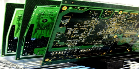
In recent years, High-Density Interconnect (HDI) multilayer PCBs have gained significant traction in the electronics industry due to their ability to support advanced electronic designs. As you explore this technology, it’s important to understand that HDI multilayer PCBs are designed with a higher density of interconnections than traditional boards, allowing manufacturers to achieve a more compact layout. This is particularly beneficial for modern devices that demand small form factors without compromising functionality. By employing methods such as blind vias and buried vias, these PCBs facilitate a more efficient use of space, paving the way for intricate circuit designs that were previously unattainable.
When working with PCB manufacturing, you may often encounter diverse options offered by various PCB manufacturing companies. Each of these companies provides unique solutions tailored to specific design requirements and could vary significantly in terms of PCB manufacturing cost. As you delve into the realm of HDI technology, it’s vital to engage with a reliable partner in the PCB manufacturing business, ensuring that the integrity and performance of your designs are upheld. Understanding the advantages offered by HDI multilayer PCBs not only helps you make informed decisions but also enhances your ability to innovate in your projects. By considering factors such as layer count, via types, and overall design capabilities, you can better navigate your path through today’s complex electronic landscape.
Key Features of HDI Technology
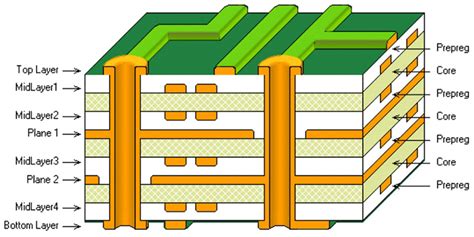
High-Density Interconnect (HDI) multilayer PCBs are designed to meet demanding requirements of modern electronic devices, thanks to their unparalleled capabilities. One of the standout features of HDI technology is the use of blind and buried vias, which allow for more complex routing in a compact space. These specialized vias are critical in facilitating the miniaturization trend in electronics, where real estate on a circuit board is at a premium. Additionally, the formation of micro vias plays a significant role in enhancing interconnections while conserving space. This nuanced approach not only optimizes pcb manufacturing but also contributes to reduced pcb manufacturing cost by streamlining designs and minimizing excess material. It’s worth noting that collaborating with reputable pcb manufacturing companies can further enhance your design capabilities, ensuring that you leverage the full potential of HDI PCBs for your applications. As you navigate the landscape of pcb manufacturing business, understanding these key features can empower you to create advanced designs that meet performance benchmarks while remaining cost-effective. In a competitive market, embracing these technological advancements in your projects can set you apart as an innovator in electronic design.
Advantages of Blind and Buried Vias
One of the significant advantages of using blind and buried vias in HDI multilayer PCBs is their contribution to enhanced design density. By allowing multiple layers of connections within a PCB, these vias facilitate a more compact layout, which is particularly advantageous in modern electronic devices where space is at a premium. The use of these advanced via types minimizes the need for traditional through-hole technology, reducing the overall PCB manufacturing cost while simultaneously enhancing electrical performance. This results in a significant decrease in the physical footprint of your design, making it possible to achieve intricate routing without compromising on functionality.
Moreover, leveraging blind and buried vias helps streamline the pcb manufacturing business process by enabling faster production cycles. As these vias decrease the number of required layers, manufacturers can optimize their workflow and resource allocation. This optimization leads to lower costs and improved turnaround times, factors that are vital for companies competing in high-demand markets. Additionally, since pcb manufacturing companies often focus on quality and reliability, utilizing advanced via technologies can help maintain high standards in performance while meeting rigorous industry specifications.
Finally, as technology continues to evolve, the incorporation of these vias into your designs will ensure that you stay ahead of emerging trends. By investing in products that utilize such sophisticated features, you not only enhance your product’s capabilities but also position yourself favorably within an increasingly competitive landscape. In conclusion, adopting blind and buried vias can make all the difference by providing substantial benefits related to compactness and performance without escalating costs excessively.
The Role of Micro Vias in Compact Designs
The advent of HDI multilayer PCBs has revolutionized the way you approach compact designs in electronics. At the core of these advanced printed circuit boards lies the technology of micro vias, which are crucial for efficient space utilization. Unlike traditional vias, micro vias can connect multiple layers in your PCB design without consuming excessive surface area. This feature is particularly beneficial when you consider that your designs need to meet the demands for smaller, more powerful electronic devices.
Micro vias, which are typically less than 150 micrometers in diameter, allow for a higher density of traces and pads, contributing to a significant reduction in overall board size while improving performance. Incorporating blind and buried vias further enhances routing options, enabling more intricate connections without the need for larger PCB space. This technique not only optimizes signal integrity but also minimizes pcb manufacturing cost by reducing material usage while maximizing functionality.
Furthermore, as you explore solutions from various pcb manufacturing companies, knowing how these techniques contribute to advanced design capabilities can set your projects apart. The benefits are clear: with carefully implemented micro vias, your designs can push the boundaries of what is achievable, ensuring that you remain competitive in a rapidly evolving market focused on miniaturization and refinement of electronic applications. Understanding this role will guide your decisions throughout the pcb manufacturing business, leading to innovative and effective solutions tailored to modern demands.
Performance Benefits of HDI Multilayer PCBs
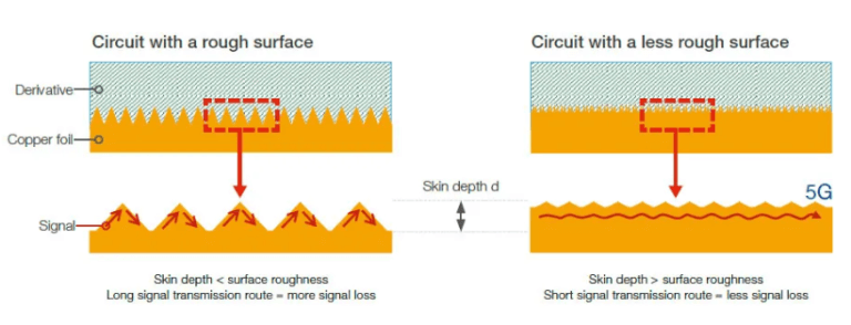
When you consider the performance benefits of HDI multilayer PCBs, it’s essential to recognize how these advanced designs cater to the evolving needs of modern electronics. One of the primary advantages is their ability to achieve higher density interconnects, which allows for more functionality in a smaller footprint. This compactness not only enhances the performance of devices but also leads to improved signal integrity and reduced latency, which are crucial in applications requiring rapid data processing. Additionally, the utilization of blind and buried vias minimizes space usage while maintaining electrical performance, significantly influencing pcb manufacturing costs positively. As a result, many pcb manufacturing companies are increasingly adopting HDI technology in their designs, driving innovation across various sectors such as consumer electronics, telecommunications, and automotive industries. This shift not only optimizes your pcb manufacturing business but also meets consumer demand for sleek and efficient devices without compromising quality or performance. Therefore, integrating these sophisticated features into your PCB designs can lead you toward a competitive advantage in an ever-evolving market landscape.
Applications of HDI Technology in Modern Electronics
The implementation of HDI multilayer PCBs has revolutionized the landscape of modern electronics by enabling innovative applications across various industries. As you explore the potential of HDI technology, consider how it enhances performance and functionality in devices such as smartphones, tablets, and medical equipment. Advanced designs utilize blind and buried vias, which not only save space but also facilitate complex routing. This ability to create more compact layouts is crucial for manufacturers looking to optimize devices without compromising on performance.
Moreover, pcb manufacturing companies are increasingly adopting these designs to meet the demands for smaller, faster, and more efficient products. The intricate nature of HDI multilayer PCBs leads to a notable reduction in pcb manufacturing cost while enhancing signal integrity, which is vital for high-frequency applications. The pcb manufacturing business can greatly benefit from these advancements, allowing for quicker turnarounds and more flexible design options. By leveraging HDI technology, you can position your products at the forefront of innovation in a competitive market, driving further adoption across various sectors such as telecommunications and automotive systems.
Design Considerations for HDI PCBs
When embarking on the journey of HDI multilayer PCB design, it is essential to consider several factors that influence efficacy and cost-effectiveness. One of the primary aspects is the pcb manufacturing process, which can vary significantly based on the complexity and design requirements of your project. Choosing the right pcb manufacturing companies can streamline the process, ensuring that you have access to advanced technologies and materials that optimize performance. Additionally, understanding the pcb manufacturing cost is crucial; as HDI designs often involve intricate features such as blind and buried vias, anticipating these costs early can prevent budget overruns.
It’s also essential to evaluate your specific needs against current trends in pcb manufacturing business, as this information allows you to align your design goals with market capabilities. When you incorporate miniaturized components into your designs, be mindful of how they integrate with traditional fabrication methods. Considering these elements will enhance not just the functionality but also the reliability and efficiency of your HDI PCBs in modern applications. Remember that thoughtful design choices today will resonate through the entire lifecycle of your electronic products, making it worthwhile to invest time in these considerations.
Future Trends in HDI Multilayer PCB Development
As the demand for high-performance electronic devices continues to grow, advancements in HDI multilayer PCBs are becoming increasingly vital in the pcb manufacturing industry. PCB manufacturing companies are now focusing on integrating innovative techniques that enhance the efficiency and functionality of their products. One trend you might observe is the ongoing miniaturization of components, leading to a greater reliance on advanced features such as blind and buried vias. This trend not only addresses space constraints but also significantly reduces the pcb manufacturing cost by optimizing material usage and simplifying assembly processes.
Moreover, with the rise of Internet of Things (IoT) devices and wearables, you can expect to see increased customization in HDI designs tailored for specific applications. Such specialization often drives pcb manufacturing business models towards agility and responsiveness to client needs, fostering collaborations between manufacturers and designers. Additionally, incorporating advancements like artificial intelligence in design processes will likely elevate overall performance and yield rates in HDI multilayer PCB production. As a result, keeping abreast of these trends will be crucial for anyone involved in designing or producing modern electronic devices, ensuring you harness the full potential of HDI technology while staying competitive in a rapidly evolving market.
Conclusion
In summary, HDI multilayer PCBs represent a significant advancement in the realm of printed circuit boards, combining intricate design capabilities with performance benefits that are essential for today’s compact electronic devices. Their reliance on features such as blind and buried vias allows for a reduction in the overall size of circuits while maintaining a high level of functionality. By investing in HDI technology, you can make the most out of your pcb manufacturing processes, driving efficiency and minimizing both space and material costs. For businesses engaged in the pcb manufacturing business, understanding these modern techniques can be crucial for staying competitive in a rapidly evolving market. Moreover, collaboration with specialized pcb manufacturing companies can provide insights into optimizing your design strategies and managing the pcb manufacturing cost, ensuring that you achieve the desired performance metrics without compromising on quality. By embracing these innovations, you pave the way for enhanced product development and engineering excellence in your projects.
FAQs
What are HDI multilayer PCBs?
HDI multilayer PCBs (High-Density Interconnect multilayer Printed Circuit Boards) are advanced circuit boards that feature a greater density of interconnections, allowing for more functionality in a smaller space. This is achieved through advanced manufacturing processes that include blind and buried vias.
What advantages do HDI multilayer PCBs offer over traditional PCBs?
The primary advantages of HDI PCBs include enhanced compactness, improved electrical performance, and the ability to support higher pin counts. These benefits are crucial for meeting the demands of modern electronic devices. Additionally, the use of micro vias contributes to more efficient space utilization and signal integrity.
How does PCB manufacturing influence design options?
The pcb manufacturing process significantly impacts your design options. By understanding the capabilities offered by various pcb manufacturing companies, you can better tailor your design to utilize techniques like blind vias, which create opportunities for more complex layouts without increasing size.
What factors affect PCB manufacturing cost?
Several factors can influence the pcb manufacturing cost, including complexity of the design, material specifications, layer count, and production volume. A well-planned design can help to minimize costs while maximizing performance.
Where can I learn more about PCB manufacturing?
For comprehensive insights into the pcb manufacturing business, consider resources that outline various aspects of design and production strategies. For further information on how to optimize your PCB projects, please click here.