Understanding PCB Fiducial Marks: A Comprehensive Guide
Introduction
Printed Circuit Boards (PCBs) are the backbone of modern electronics, serving as the foundation for virtually all electronic devices. As the complexity of electronic designs increases, so does the need for precision in the manufacturing and assembly processes. One critical aspect of ensuring this precision is the use of fiducial marks. Fiducial marks, often referred to simply as fiducials, are small, precisely placed markers on a PCB that serve as reference points for automated assembly equipment. This article delves into the importance of fiducial marks, their types, design considerations, and their role in the PCB assembly process.
What Are PCB Fiducial Marks?
Fiducial marks are small, circular or cross-shaped features etched onto the surface of a PCB. These marks are typically made of copper and are often coated with a solder mask to protect them from oxidation. The primary purpose of fiducial marks is to provide a reference point for automated assembly machines, such as pick-and-place machines, solder paste printers, and optical inspection systems. By aligning these machines to the fiducial marks, manufacturers can ensure that components are placed accurately and that the solder paste is applied precisely.
Fiducial marks are especially important in high-density PCB designs, where even minor misalignments can lead to significant issues, such as short circuits, open connections, or improperly soldered components. In such cases, fiducial marks act as a guide, enabling the assembly equipment to compensate for any slight variations in the PCB’s position or orientation.

Types of Fiducial Marks
There are two main types of fiducial marks used in PCB design: global fiducials and local fiducials.
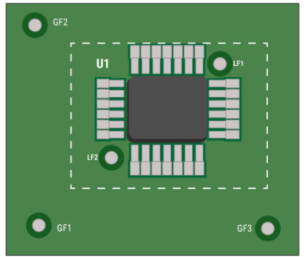
- Global Fiducials: Global fiducials are placed on the outer edges of the PCB and are used to align the entire board during the assembly process. These fiducials are typically located near the corners of the PCB, although their exact placement may vary depending on the design and the requirements of the assembly equipment. Global fiducials are essential for ensuring that the entire board is properly aligned before any components are placed.
- Local Fiducials: Local fiducials are placed near specific components or groups of components that require particularly high precision during placement. These fiducials are used in addition to global fiducials and provide an additional layer of accuracy for critical components, such as fine-pitch integrated circuits (ICs) or ball grid array (BGA) packages. Local fiducials are especially important in designs where tight tolerances are required, as they allow the assembly equipment to make fine adjustments to the placement of individual components.
Design Considerations for Fiducial Marks
When designing a PCB, several factors must be considered to ensure that the fiducial marks are effective and reliable. These considerations include the size, shape, placement, and clearance of the fiducial marks.
- Size and Shape: Fiducial marks are typically circular, with a diameter ranging from 1mm to 3mm. The size of the fiducial mark should be large enough to be easily detected by the assembly equipment’s vision system but not so large that it interferes with the placement of nearby components. The shape of the fiducial mark is also important, as circular marks are generally easier for vision systems to detect and align with than other shapes.
- Placement: The placement of fiducial marks is critical to their effectiveness. Global fiducials should be placed near the corners of the PCB, with at least two fiducials on opposite corners to provide a reference for both the X and Y axes. Local fiducials should be placed near the components they are intended to align, typically within a few millimeters of the component’s center. It is important to ensure that fiducial marks are placed in areas that are free from obstructions, such as other components or traces, to ensure that they can be easily detected by the assembly equipment.
- Clearance: Fiducial marks should have adequate clearance from other features on the PCB, such as components, traces, and vias. This clearance ensures that the fiducial marks are not obscured or interfered with during the assembly process. A common rule of thumb is to provide a clearance of at least 1mm around each fiducial mark, although this may vary depending on the specific requirements of the assembly equipment.
- Solder Mask and Surface Finish: Fiducial marks are typically made of copper and are often coated with a solder mask to protect them from oxidation. However, the solder mask should not cover the fiducial mark itself, as this would make it difficult for the assembly equipment’s vision system to detect the mark. Additionally, the surface finish of the fiducial mark should be chosen carefully to ensure that it provides a high contrast with the surrounding PCB material, making it easier for the vision system to detect.
The Role of Fiducial Marks in the PCB Assembly Process
Fiducial marks play a crucial role in the PCB assembly process, particularly in automated assembly lines. The following sections outline the key steps in the assembly process where fiducial marks are used.
- Solder Paste Printing: The first step in the PCB assembly process is the application of solder paste to the PCB. This is typically done using a stencil printer, which applies solder paste to the pads where components will be placed. The stencil printer uses the global fiducial marks to align the stencil with the PCB, ensuring that the solder paste is applied accurately. If the stencil is misaligned, the solder paste may be applied to the wrong areas, leading to defects such as solder bridges or insufficient solder joints.
- Component Placement: After the solder paste has been applied, the next step is to place the components onto the PCB. This is done using a pick-and-place machine, which uses the global fiducial marks to align the PCB and ensure that components are placed accurately. For components that require high precision, such as fine-pitch ICs or BGAs, the pick-and-place machine may also use local fiducial marks to make fine adjustments to the component’s placement.
- Reflow Soldering: Once the components have been placed, the PCB is passed through a reflow oven, where the solder paste is melted to form permanent solder joints. During this process, the fiducial marks are not directly used, but their accurate placement during the previous steps ensures that the components remain in the correct position as the solder paste melts and solidifies.
- Optical Inspection: After the reflow soldering process, the PCB is typically inspected using an automated optical inspection (AOI) system. The AOI system uses the fiducial marks to align the PCB and ensure that the inspection is performed accurately. The AOI system checks for defects such as misaligned components, solder bridges, or insufficient solder joints, and any issues are flagged for further inspection or rework.
Challenges and Best Practices
While fiducial marks are essential for ensuring the accuracy of the PCB assembly process, there are several challenges that designers and manufacturers must be aware of. These challenges include:
- Variability in PCB Manufacturing: Even with precise design and manufacturing processes, there can be slight variations in the size, shape, and placement of fiducial marks. These variations can be caused by factors such as thermal expansion, etching tolerances, or inconsistencies in the solder mask application. To mitigate these issues, it is important to design fiducial marks with sufficient tolerance and to use high-quality manufacturing processes.
- Vision System Limitations: The effectiveness of fiducial marks depends on the ability of the assembly equipment’s vision system to detect and align with them. However, vision systems can be affected by factors such as lighting conditions, reflections, or obstructions on the PCB. To ensure reliable detection, fiducial marks should be designed with high contrast and placed in areas that are free from obstructions.
- Component Density: In high-density PCB designs, there may be limited space available for fiducial marks. In such cases, it is important to carefully balance the need for fiducial marks with the need to place components as close together as possible. One approach is to use smaller fiducial marks or to place them in areas that are less critical for component placement.
Conclusion
Fiducial marks are a critical component of the PCB design and assembly process, providing the reference points needed for accurate and reliable assembly. By understanding the types of fiducial marks, their design considerations, and their role in the assembly process, designers and manufacturers can ensure that their PCBs are assembled with the highest level of precision. As electronic designs continue to become more complex, the importance of fiducial marks will only continue to grow, making them an essential tool for anyone involved in the PCB industry.

