Understanding PCB Impedance: Definition, Importance, and Control
Introduction to PCB Impedance
Printed Circuit Board (PCB) impedance is a fundamental concept in modern electronics design that has become increasingly critical as signal speeds continue to rise. Impedance, measured in ohms (Ω), represents the total opposition that a circuit presents to alternating current (AC) or signal propagation. In PCB contexts, impedance specifically refers to the characteristic impedance of transmission lines formed by PCB traces and their reference planes.
As electronic devices operate at higher frequencies—with modern systems routinely handling signals in the gigahertz range—proper impedance control has transitioned from a specialized requirement to a standard design consideration. This article will explore the definition of PCB impedance, its various types, calculation methods, and the practical aspects of impedance control in PCB manufacturing.
The Fundamental Definition of PCB Impedance
PCB impedance, more precisely called characteristic impedance (Z₀), is defined as the ratio of voltage to current in a propagating electromagnetic wave traveling along a transmission line structure on the PCB. Mathematically, it’s expressed as:
Z₀ = √(L/C)
Where:
- Z₀ is the characteristic impedance
- L is the distributed inductance per unit length
- C is the distributed capacitance per unit length
This definition reveals that PCB impedance is an inherent property of the physical structure of the transmission line, determined by its geometry and the materials used, rather than being dependent on the line’s length.
In practical PCB terms, impedance arises from the interaction between:
- Signal traces (typically copper)
- Dielectric material (the PCB substrate, usually FR-4)
- Reference planes (ground or power planes)
- Other nearby conductors

Types of PCB Impedance
1. Single-Ended Impedance
This refers to the characteristic impedance of a single trace relative to its reference plane. It’s the most basic form of PCB impedance and is relevant for single-ended signaling schemes.
2. Differential Impedance
Critical for differential signaling (like USB, HDMI, PCI Express), differential impedance is the impedance between two complementary signal traces that carry opposite-phase signals. It’s not simply twice the single-ended impedance due to coupling effects between the pair.
3. Common Mode Impedance
This measures the impedance of both lines in a differential pair when driven with identical signals relative to ground.
4. Odd Mode and Even Mode Impedance
These more advanced concepts describe impedance characteristics when differential pairs are excited with specific signal patterns, important for precise analysis of coupled transmission lines.
Factors Affecting PCB Impedance
Several geometric and material factors determine the impedance of PCB traces:
- Trace Width: Wider traces lower impedance (more capacitive coupling), narrower traces increase impedance.
- Trace Thickness: Thicker copper increases impedance slightly by reducing resistance.
- Dielectric Thickness: Greater distance to reference plane increases impedance.
- Dielectric Constant (Dk or εᵣ): Materials with higher Dk lower impedance.
- Solder Mask: Can slightly affect impedance by changing effective dielectric properties.
- Frequency: Impedance can vary with frequency due to material dispersion.
Impedance Calculation Methods
1. Microstrip Transmission Lines
Common for outer layers, where a trace runs over a reference plane with dielectric below and air above. The impedance depends on the trace geometry and the effective dielectric constant.
2. Stripline Transmission Lines
Used for inner layers, where a trace is embedded between two reference planes with dielectric material all around. Offers better shielding but typically lower impedance than microstrip.
3. Coplanar Waveguide
Features a trace with adjacent ground planes on the same layer, offering good high-frequency performance.
Numerical methods and field solvers are typically used for precise impedance calculations, though simplified formulas exist for basic estimations.
Importance of Impedance Control
Proper impedance control is essential because:
- Signal Integrity: Mismatched impedance causes reflections that distort signals.
- Power Transfer: Maximum power transfer occurs when impedances match.
- EMI Reduction: Controlled impedance minimizes unintended radiation.
- Timing Accuracy: Impedance affects propagation delay and signal timing.
- System Reliability: Consistent impedance prevents intermittent faults.
In high-speed designs (generally >50MHz or rise times <1ns), impedance control becomes mandatory rather than optional.
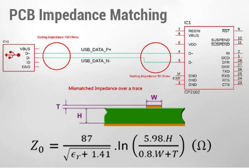
PCB Impedance Specifications
Impedance requirements are typically specified as:
- Target value (e.g., 50Ω single-ended, 100Ω differential)
- Tolerance (usually ±10%, ±5% for more critical applications)
- Applicable frequency range
Common standard impedance values include:
- 50Ω: Common for RF systems and single-ended general purpose
- 75Ω: Used in video applications
- 100Ω: Standard for differential pairs (USB, Ethernet, etc.)
- 90Ω: Sometimes used for differential signaling
Impedance Measurement and Verification
Several methods exist to verify PCB impedance:
- Time Domain Reflectometry (TDR): The gold standard, sending pulses and measuring reflections.
- Network Analysis: Frequency domain measurements using VNAs.
- Calculated Verification: Using precise measurements of physical parameters.
- Test Coupons: Special test structures on panel edges for destructive testing.
Manufacturing Considerations
Achieving consistent impedance in production requires:
- Material Control: Consistent dielectric properties and copper quality.
- Process Control: Precise etching, lamination, and thickness control.
- Design for Manufacturability: Accounting for manufacturing tolerances.
- Testing: Regular impedance verification during production.
Challenges in PCB Impedance Control
Designers and manufacturers face several challenges:
- Material Variations: Dielectric constant can vary between batches.
- Manufacturing Tolerances: Etching undercuts, layer-to-layer misregistration.
- Frequency Effects: Material properties change with frequency.
- Complex Stackups: Managing impedance in multilayer boards with mixed signaling.
- Surface Roughness: Affects loss and effective impedance at high frequencies.
Advanced Topics in PCB Impedance
1. Frequency-Dependent Effects
At very high frequencies (>10GHz), additional factors become significant:
- Skin effect (current crowding at conductor surfaces)
- Dielectric loss
- Surface roughness effects
2. Anisotropic Materials
Some advanced PCB materials have different dielectric properties in different directions.
3. Impedance Discontinuities
Vias, connectors, and transitions often create impedance variations that must be managed.
4. Mixed Dielectric Environments
Modern PCBs often combine multiple materials with different properties.
Best Practices for PCB Impedance Control
- Early Collaboration: Involve your PCB manufacturer during design.
- Conservative Design: Allow margin for manufacturing variations.
- Clear Specifications: Document all impedance requirements clearly.
- Use Appropriate Tools: Employ proper field-solving software for calculations.
- Test Verification: Include test structures for impedance verification.
Future Trends in PCB Impedance Control
As electronics continue advancing, impedance control faces new challenges:
- Higher frequencies (5G, millimeter-wave applications)
- More complex materials (low-loss, high-frequency substrates)
- 3D packaging and advanced interconnects
- Automated impedance tuning and adaptive matching
Conclusion
PCB impedance is a complex but crucial aspect of modern electronic design that bridges the gap between theoretical circuit requirements and physical implementation. Proper understanding and control of impedance enables reliable high-speed signal transmission, reduces electromagnetic interference, and ensures overall system performance. As signal speeds continue increasing, the importance of precise impedance control will only grow, requiring designers and manufacturers to maintain rigorous attention to material properties, geometric tolerances, and measurement methodologies. By mastering PCB impedance concepts, engineers can create more robust, higher-performing electronic systems capable of meeting the demands of tomorrow’s technologies.