Understanding PCB Propagation Delay: Causes, Effects, and Mitigation Strategies
In the realm of high-speed electronics, signal integrity is a critical concern for designers and engineers. One of the key factors affecting signal integrity is propagation delay, which refers to the time it takes for a signal to travel from one point on a printed circuit board (PCB) to another. As electronic devices continue to operate at higher frequencies and faster data rates, understanding and managing propagation delay has become essential for ensuring reliable performance. This article explores the concept of PCB propagation delay, its causes, effects, and strategies to mitigate its impact.
What Is Propagation Delay?
Propagation delay is the time it takes for an electrical signal to travel from the transmitter to the receiver along a transmission line on a PCB. It is typically measured in picoseconds per inch (ps/in) or nanoseconds per meter (ns/m). Propagation delay is influenced by the physical properties of the PCB materials and the design of the transmission lines.
In high-speed digital circuits, even small delays can lead to timing errors, signal degradation, and reduced system performance. Therefore, managing propagation delay is crucial for maintaining signal integrity and ensuring that devices operate as intended.
Key Factors Influencing Propagation Delay
Propagation delay is determined by several factors, including the dielectric constant of the PCB material, the geometry of the transmission lines, and the operating frequency. Understanding these factors is essential for designing PCBs that meet performance requirements.
1. Dielectric Constant (Dk)
- The dielectric constant, or relative permittivity, of the PCB material affects the speed at which signals propagate. A higher dielectric constant results in slower signal propagation and increased delay.
- Common PCB materials, such as FR-4, have a dielectric constant of around 4.2 to 4.5, while high-frequency materials like Rogers laminates have lower dielectric constants (e.g., 2.2 to 3.5).
2. Transmission Line Geometry
- The width, thickness, and spacing of the traces on a PCB influence the characteristic impedance and propagation delay.
- Microstrip and stripline are the two most common transmission line configurations. Microstrip traces are on the outer layers of the PCB, while stripline traces are embedded between two ground planes. Stripline configurations generally have higher propagation delays due to the surrounding dielectric material.
3. Operating Frequency
- At higher frequencies, signals are more susceptible to delays and distortions caused by the PCB materials and trace geometry.
- High-frequency signals also experience greater losses, which can exacerbate the effects of propagation delay.
4. Trace Length
- Longer traces inherently have greater propagation delays. In high-speed designs, minimizing trace lengths is essential to reduce delay and maintain signal integrity.
5. Temperature and Environmental Conditions
- Temperature variations can affect the dielectric constant of the PCB material, leading to changes in propagation delay.
- Environmental factors such as humidity and mechanical stress can also impact signal propagation.
Effects of Propagation Delay
Propagation delay can have several adverse effects on the performance of electronic systems, particularly in high-speed and high-frequency applications. Some of the key effects include:
- Timing Errors:
- In digital circuits, propagation delay can cause timing mismatches between signals, leading to errors in data transmission and processing.
- For example, in synchronous systems, clock skew caused by propagation delay can result in setup and hold time violations.
- Signal Degradation:
- Delays can cause signal reflections, ringing, and crosstalk, which degrade signal quality and reduce the reliability of the system.
- In high-frequency applications, these effects can lead to data corruption and increased bit error rates.
- Reduced Bandwidth:
- Propagation delay limits the maximum achievable data rate and bandwidth of a system.
- In high-speed communication systems, such as Ethernet or PCIe, excessive delay can reduce the effective data throughput.
- Increased Power Consumption:
- To compensate for delays, designers may need to increase the drive strength of signals, which can lead to higher power consumption and heat generation.
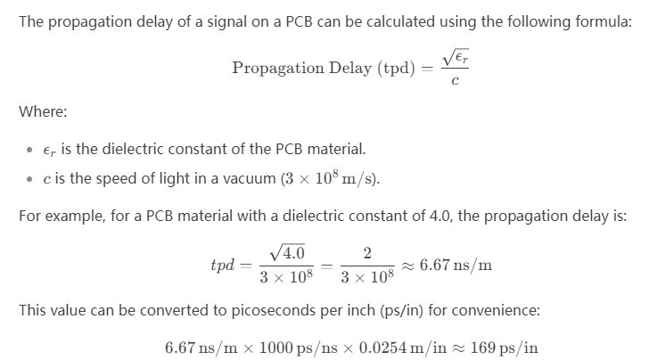
Calculating Propagation Delay
Mitigation Strategies for Propagation Delay
To minimize the impact of propagation delay on PCB performance, designers can employ several strategies:
1. Material Selection
- Use PCB materials with low dielectric constants to reduce propagation delay. High-frequency materials like Rogers laminates are ideal for high-speed applications.
- Consider the temperature stability of the material to ensure consistent performance under varying conditions.
2. Optimize Trace Geometry
- Use controlled impedance traces to match the characteristic impedance of the transmission lines to the source and load impedances.
- Minimize trace lengths, especially for high-speed signals, to reduce delay and signal degradation.
3. Layer Stackup Design
- Use stripline configurations for critical high-speed signals to provide better shielding and reduce crosstalk.
- Ensure proper spacing between signal layers and ground planes to minimize impedance variations.
4. Signal Integrity Analysis
- Perform signal integrity simulations during the design phase to identify potential issues related to propagation delay.
- Use tools like SPICE or electromagnetic simulation software to model signal behavior and optimize trace routing.
5. Equalization and Pre-Emphasis
- In high-speed communication systems, use equalization and pre-emphasis techniques to compensate for signal degradation caused by propagation delay.
- These techniques can help restore signal integrity and improve data transmission rates.
6. Clock Distribution Networks
- Design clock distribution networks with matched trace lengths to minimize clock skew and ensure synchronous operation.
- Use techniques such as clock tree synthesis and delay matching to achieve precise timing.
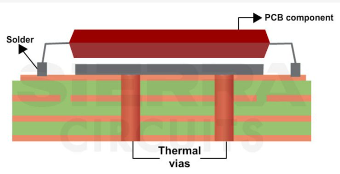
7. Thermal Management
- Implement effective thermal management strategies to maintain stable operating temperatures and prevent variations in propagation delay.
- Use thermal vias, heat sinks, and proper airflow to dissipate heat efficiently.
Applications and Case Studies
Propagation delay is a critical consideration in various high-speed and high-frequency applications. Here are some examples:
- High-Speed Digital Circuits:
- In CPUs, GPUs, and FPGAs, propagation delay affects the timing of clock signals and data paths.
- Designers use advanced routing techniques and low-Dk materials to minimize delays and ensure reliable operation.
- Communication Systems:
- In Ethernet, PCIe, and USB interfaces, propagation delay impacts data transmission rates and signal integrity.
- Equalization and pre-emphasis techniques are commonly used to mitigate delay-related issues.
- RF and Microwave Systems:
- In RF and microwave circuits, propagation delay affects the phase and amplitude of signals.
- Designers use high-frequency materials and precise trace geometries to achieve the desired performance.
- Aerospace and Defense:
- In radar and satellite systems, propagation delay can impact the accuracy and reliability of signal processing.
- Advanced materials and thermal management techniques are employed to address these challenges.
Challenges and Future Trends
As electronic systems continue to push the boundaries of speed and performance, managing propagation delay will remain a significant challenge. Some of the key trends and challenges include:
- Higher Data Rates:
- The demand for faster data rates in applications like 5G, AI, and IoT will require even lower propagation delays and improved signal integrity.
- Advanced Materials:
- The development of new PCB materials with ultra-low dielectric constants and improved thermal stability will play a crucial role in addressing propagation delay.
- 3D and Heterogeneous Integration:
- The rise of 3D packaging and heterogeneous integration introduces new challenges for managing propagation delay in complex, multi-layer designs.
- Machine Learning and AI:
- The use of machine learning and AI in PCB design tools can help optimize trace routing and minimize propagation delay.
Conclusion
Propagation delay is a critical factor in the design of high-speed and high-frequency PCBs. By understanding the causes and effects of propagation delay and implementing effective mitigation strategies, designers can ensure reliable performance and signal integrity in their electronic systems.
As technology continues to evolve, the importance of managing propagation delay will only increase. By leveraging advanced materials, design techniques, and simulation tools, engineers can meet the challenges of modern electronics and enable the next generation of innovative devices. Whether you’re designing cutting-edge communication systems or high-performance computing platforms, mastering the intricacies of propagation delay is essential for success.