Understanding Top Overlay in PCB Design: A Comprehensive Guide
In the world of printed circuit board (PCB) design, the top overlay (also known as the silkscreen layer) plays a crucial role in ensuring the functionality, manufacturability, and usability of the final product. The top overlay is a layer of text, symbols, and markings printed on the surface of the PCB, typically using epoxy ink. It provides essential information for assembly, testing, and debugging, making it an indispensable part of the PCB design process. This article explores the purpose, design considerations, and best practices for the top overlay in PCB design.
What Is the Top Overlay?
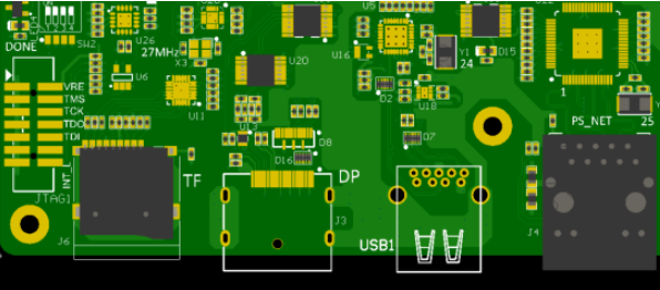
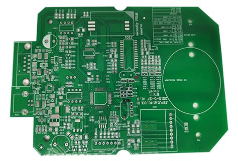
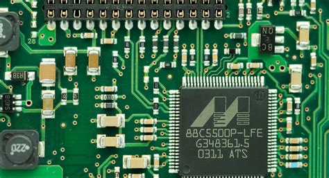
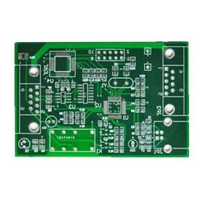
The top overlay is a non-conductive layer on the PCB that contains human-readable information such as component designators, polarity markings, test points, and logos. It is usually printed in white, although other colors like yellow or black may be used depending on the PCB’s solder mask color. The top overlay serves several key purposes:
- Component Identification: Labels such as “R1” for resistors or “C2” for capacitors help assemblers place components correctly.
- Polarity and Orientation Markings: Symbols like “+” or “-” indicate the correct orientation of polarized components such as diodes, capacitors, and ICs.
- Test Points and Debugging: Labels for test points and debugging pads make it easier to diagnose and troubleshoot the PCB.
- Manufacturer Information: Logos, part numbers, and revision codes provide traceability and branding.
- User Guidance: Instructions or warnings (e.g., “High Voltage”) help users interact with the PCB safely and effectively.
Importance of the Top Overlay in PCB Design
The top overlay is more than just a cosmetic feature; it is a functional layer that enhances the usability and reliability of the PCB. Here are some reasons why the top overlay is important:
- Assembly Accuracy: Clear and accurate markings reduce the risk of errors during component placement, especially in manual or semi-automated assembly processes.
- Debugging and Testing: Well-labeled test points and debugging pads simplify the process of diagnosing and repairing the PCB.
- User Safety: Warnings and instructions on the top overlay help prevent accidents, such as incorrect connections or exposure to high-voltage areas.
- Traceability: Part numbers, revision codes, and manufacturer logos provide essential information for quality control and inventory management.
- Aesthetic Appeal: A clean and professional-looking top overlay enhances the overall appearance of the PCB, which can be important for consumer-facing products.
Design Considerations for the Top Overlay
Designing an effective top overlay requires careful planning and attention to detail. Here are some key considerations:
1. Legibility
- Font Size and Style: Use a font size that is large enough to be readable but small enough to fit within the available space. Sans-serif fonts like Arial or Verdana are commonly used for their clarity.
- Contrast: Ensure that the overlay color contrasts well with the solder mask color. For example, white overlay on green solder mask is a popular combination.
2. Placement
- Component Designators: Place designators (e.g., “R1,” “C2”) close to their corresponding components but avoid overlapping pads or vias.
- Polarity Markings: Clearly indicate the polarity of components such as diodes, capacitors, and ICs.
- Test Points: Label test points and debugging pads for easy identification during testing and troubleshooting.
3. Avoiding Obstructions
- Solder Mask Openings: Ensure that the overlay does not overlap with solder mask openings, as this can cause ink to bleed into exposed copper areas.
- Component Footprints: Avoid placing overlay text under components, as it may become obscured or interfere with soldering.
4. Manufacturing Constraints
- Minimum Line Width: Check the manufacturer’s specifications for the minimum line width and spacing for the overlay. Typical values are around 0.15 mm for line width and 0.2 mm for spacing.
- Ink Thickness: Be aware that the overlay ink has a finite thickness, which can affect the clearance between the overlay and components.
5. Revision Control
- Include revision codes or dates on the overlay to track changes and ensure that the correct version of the PCB is being used.
6. Aesthetic Considerations
- Alignment and Symmetry: Align text and symbols neatly to create a professional appearance.
- Logos and Branding: Incorporate logos or branding elements if desired, but ensure they do not interfere with functional markings.
Best Practices for Top Overlay Design
To create an effective and manufacturable top overlay, follow these best practices:
- Use Consistent Naming Conventions:
- Adopt a consistent naming scheme for component designators (e.g., “R” for resistors, “C” for capacitors, “U” for ICs).
- Prioritize Critical Information:
- Place the most important information, such as polarity markings and test points, in prominent locations.
- Minimize Overlay Text:
- Avoid cluttering the overlay with unnecessary text or symbols. Focus on providing clear and concise information.
- Verify Clearances:
- Use design rule checks (DRC) to ensure that the overlay does not overlap with pads, vias, or component footprints.
- Collaborate with Manufacturers:
- Consult with your PCB manufacturer to understand their capabilities and limitations for overlay printing.
- Test for Legibility:
- Print a sample of the overlay at actual size to verify that all text and symbols are legible.
- Consider Future Revisions:
- Leave space for additional markings or revisions that may be required in future iterations of the PCB.
Common Mistakes to Avoid
Even experienced designers can make mistakes when creating the top overlay. Here are some common pitfalls to watch out for:
- Overlapping Pads or Vias:
- Overlay text that overlaps with pads or vias can cause manufacturing issues and reduce legibility.
- Incorrect Polarity Markings:
- Mislabeling the polarity of components can lead to assembly errors and PCB failures.
- Insufficient Contrast:
- Poor contrast between the overlay and solder mask colors can make the text difficult to read.
- Overcrowding:
- Adding too much information to the overlay can make it cluttered and hard to interpret.
- Ignoring Manufacturer Guidelines:
- Failing to adhere to the manufacturer’s specifications for line width, spacing, and ink thickness can result in a subpar overlay.
Tools and Software for Top Overlay Design
Modern PCB design software provides powerful tools for creating and managing the top overlay. Some popular options include:
- Altium Designer:
- Offers advanced features for overlay design, including automatic component labeling and design rule checks.
- KiCad:
- A free and open-source tool with robust overlay design capabilities.
- Eagle:
- Provides easy-to-use tools for creating and editing the top overlay.
- OrCAD:
- Includes features for precise control over overlay text and symbols.
- PADS:
- Offers comprehensive tools for managing all aspects of PCB design, including the top overlay.
Applications of the Top Overlay
The top overlay is used in a wide range of PCB applications, including:
- Consumer Electronics:
- Smartphones, tablets, and laptops use the top overlay for component identification and branding.
- Industrial Equipment:
- Control systems and machinery rely on the top overlay for debugging and maintenance.
- Medical Devices:
- Medical PCBs use the top overlay to ensure accurate assembly and user safety.
- Automotive Electronics:
- Automotive PCBs include overlay markings for polarity, test points, and part numbers.
- Aerospace and Defense:
- High-reliability PCBs in aerospace and defense applications use the top overlay for traceability and debugging.
Conclusion
The top overlay is a vital component of PCB design, providing essential information for assembly, testing, and debugging. By following best practices and avoiding common mistakes, designers can create clear, accurate, and professional-looking overlays that enhance the functionality and usability of their PCBs.
As PCB technology continues to evolve, the importance of the top overlay will remain unchanged. Whether you’re designing a simple prototype or a complex multi-layer board, paying attention to the top overlay will ensure that your PCB is not only functional but also easy to assemble, test, and maintain. By leveraging modern design tools and collaborating with manufacturers, you can create top overlays that meet the highest standards of quality and reliability.