Understanding Voltage Drop in PCB Design: Causes, Effects, and Solutions
Introduction to Voltage Drop in PCBs
Voltage drop, often referred to as IR drop in PCB design, is a critical consideration that affects the performance, reliability, and functionality of electronic circuits. In simple terms, voltage drop occurs when electrical current flowing through a conductor (such as a PCB trace or plane) encounters resistance, resulting in a reduction of voltage between the power source and the load component.
This phenomenon becomes increasingly significant in modern PCB designs where:
- Power requirements continue to rise while operating voltages decrease
- High-current applications become more common
- Board sizes shrink, requiring careful power distribution planning
- High-speed digital circuits demand clean, stable power supplies
Understanding and properly managing voltage drop is essential for PCB designers to ensure their circuits operate as intended throughout the product’s lifecycle.
Fundamental Causes of Voltage Drop
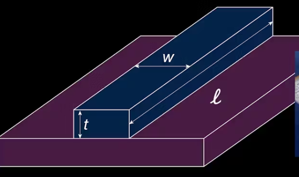
1. Trace Resistance
Every PCB trace has inherent resistance determined by three primary factors:
- Conductor material: Copper is standard, with resistivity of approximately 1.7×10⁻⁸ Ω·m at 20°C
- Cross-sectional area: Function of trace width and copper thickness (typically measured in oz/ft²)
- Trace length: Longer traces exhibit higher resistance
The resistance can be calculated using:
R = ρ × (L/A)
Where:
- R = resistance in ohms (Ω)
- ρ = resistivity of the material (Ω·m)
- L = length of the conductor (m)
- A = cross-sectional area (m²)
2. Current Demand
Ohm’s Law (V = I × R) reveals that voltage drop increases linearly with current. Modern components often have:
- Dynamic current requirements (especially digital ICs)
- High peak currents during switching
- Low-voltage operation with tight tolerance requirements
3. Plane and Via Resistance
Power planes and vias contribute to overall resistance:
- Plane resistance is typically low but can be significant for high currents
- Vias add discrete resistance points (typically 0.1-1.0Ω each)
- Poor via placement can create current bottlenecks
4. Temperature Effects
Copper resistance increases with temperature (approximately +0.4%/°C):
- Operating environment temperature
- Self-heating from current flow
- Adjacent component heating
Effects of Excessive Voltage Drop
1. Functional Problems
- Undervoltage conditions: Components may fail to operate correctly or at specified speeds
- Increased signal noise: Reduced noise margins in digital circuits
- Timing issues: Clock skew and signal integrity problems
2. Performance Degradation
- Reduced maximum clock speeds
- Decreased output drive capability
- Increased susceptibility to electromagnetic interference (EMI)
3. Reliability Concerns
- Thermal stress from increased current draw
- Accelerated electromigration in traces
- Potential for latch-up conditions in CMOS devices
4. Power Efficiency Reduction
- Wasted energy dissipated as heat
- Reduced battery life in portable devices
- Increased thermal management requirements
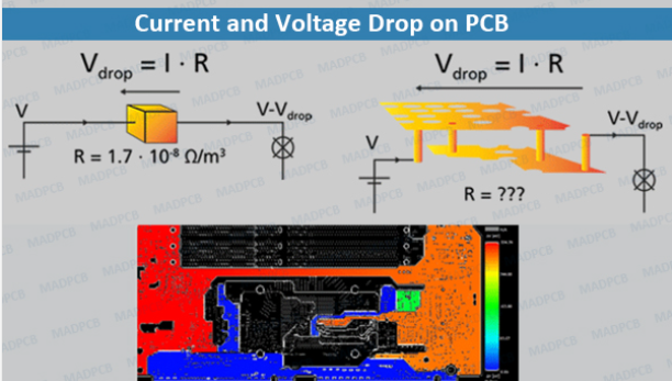
Calculating Voltage Drop in PCB Designs
Basic DC Calculations
For simple cases, use Ohm’s Law:
V_drop = I × R_trace
Where:
- I = current in amps
- R_trace = trace resistance calculated from geometry and material properties
Advanced Considerations
For more accurate analysis:
- Segment traces into sections with different geometries
- Account for temperature using:
R(T) = R₀ × [1 + α × (T – T₀)]
Where α is the temperature coefficient of resistance - Include via resistance in the total path
- Consider AC effects for high-frequency components
PCB Stackup Considerations
- Copper weight: Standard options include 0.5oz, 1oz, 2oz (thicker copper reduces resistance)
- Layer utilization: Dedicated power planes vs. routed power traces
- Dielectric materials: Affect thermal performance and heat dissipation
Design Techniques to Minimize Voltage Drop
1. Proper Trace Sizing
- Use width calculators based on current requirements
- IPC-2152 provides standards for current-carrying capacity
- Consider both DC and transient current needs
2. Power Distribution Network (PDN) Optimization
- Implement solid power planes where possible
- Use star topologies for critical power distribution
- Implement proper decoupling capacitor placement
3. Strategic Via Placement
- Use multiple vias for high-current connections
- Consider via stitching for power planes
- Optimize via size and plating thickness
4. Material Selection
- Higher copper weights for power layers
- Consider heavy copper PCBs (up to 6oz or more) for extreme cases
- Thermal management materials for high-power designs
5. Voltage Margin Design
- Design with safety margins (typically 5-10%)
- Consider worst-case operating conditions
- Account for manufacturing tolerances
Simulation and Analysis Tools
Modern PCB design incorporates several analysis methods:
1. DC Analysis Tools
- Built into most PCB design packages
- Provide visual voltage drop maps
- Highlight critical areas needing improvement
2. 3D Field Solvers
- More accurate modeling of complex geometries
- Account for proximity effects and unusual shapes
- Handle multi-layer interactions
3. Thermal Coupled Analysis
- Combined electrical and thermal simulation
- Predict temperature rise and its effect on resistance
- Identify potential hot spots
4. Frequency Domain Analysis
- Important for AC voltage drop considerations
- Analyze impedance of power delivery network
- Optimize decoupling networks
Case Studies and Practical Examples
Case Study 1: High-Current Digital Board
A 16-layer server motherboard experiencing random resets:
- Problem: 1.2V supply to processors showed 150mV drop under load
- Root cause: Inadequate via count between power planes
- Solution: Added 200 additional vias in power distribution path
- Result: Drop reduced to 35mV, stable operation achieved
Case Study 2: Automotive Control Module
Engine control unit failing in high-temperature conditions:
- Problem: 5V supply to sensors dropping to 4.6V at 85°C
- Root cause: Narrow traces with insufficient temperature margin
- Solution: Redesigned with wider traces and 2oz copper
- Result: Maintained 4.9V at 125°C, meeting specifications
Case Study 3: Portable Medical Device
Battery-powered device with premature shutdowns:
- Problem: Voltage drop in charging circuit reducing effective capacity
- Root cause: Long, thin traces from connector to battery
- Solution: Optimized routing with dedicated power layer
- Result: 12% improvement in operational time between charges
Future Trends and Challenges
1. Lower Voltage Requirements
As ICs move to smaller process nodes:
- Operating voltages continue to decrease (now below 1V for some processors)
- Tolerances become tighter (often ±3% or less)
- Makes voltage drop management more critical
2. Higher Current Demands
Modern processors and ASICs may require:
- Hundreds of amps at very low voltages
- Complex multi-phase power delivery
- Advanced cooling requirements
3. Advanced Materials
Emerging solutions include:
- Embedded bus bars for ultra-high current
- Carbon nanotube conductors
- Superconducting materials for extreme applications
4. 3D Power Delivery
With 3D IC packaging:
- Vertical power distribution challenges
- Through-silicon vias (TSVs) for power delivery
- Thermal management in stacked dies
Best Practices Summary
- Start early: Consider power distribution during initial layout planning
- Use appropriate tools: Leverage simulation capabilities in your design software
- Design with margins: Account for worst-case operating conditions
- Monitor temperatures: Remember that heat increases resistance
- Verify prototypes: Always measure actual voltage drops in physical boards
- Document standards: Create design rules for power distribution in your organization
Conclusion
Voltage drop in PCB design is a fundamental consideration that bridges electrical theory with practical implementation. As electronic systems become more power-hungry yet voltage-sensitive, proper management of IR drops becomes increasingly critical to product success. By understanding the causes, effects, and mitigation strategies discussed in this article, PCB designers can create robust power delivery networks that ensure reliable operation across all intended use cases.
The key takeaways are:
- Voltage drop results from inherent resistance in conductors carrying current
- Effects range from performance degradation to complete circuit failure
- Careful design and analysis can effectively manage voltage drop
- Modern tools provide powerful simulation capabilities
- Future trends will present new challenges requiring innovative solutions
Through thoughtful application of these principles, engineers can overcome voltage drop challenges and deliver high-quality PCB designs that meet the demanding requirements of today’s electronic products.