Unlocking Innovation: The Ultimate Guide to Custom PCB Printing
Key Takeaways
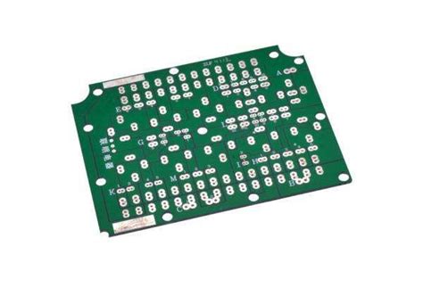
In the realm of pcb manufacturing, the significance of custom PCB printing cannot be overstated. It allows you to tailor printed circuit boards to meet your unique requirements, unlocking unparalleled innovation in electronics. Understanding the capabilities of pcb manufacturing companies helps you leverage rapid prototyping and cost-effective production techniques. These advantages not only reduce pcb manufacturing cost but also expedite the development process. Additionally, the variety of advanced materials used in custom PCB projects ensures that your creations can perform under diverse conditions. From CNC milling to laser cutting, and even 3D printing, various techniques offer you flexibility and precision in your designs. This holistic understanding of custom PCB printing sets a solid foundation for optimizing your design process and achieving superior quality in your custom projects, marking a significant milestone in the pcb manufacturing business.
Introduction to Custom PCB Printing
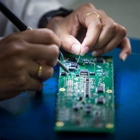
When it comes to custom PCB printing, you are entering a realm where creativity meets precise engineering. PCB manufacturing has evolved dramatically, offering you the flexibility to tailor designs that meet specific project requirements. Whether you are an engineer or a hobbyist, understanding the nuances of custom PCB printing can significantly enhance your work.
At the heart of this process is the design stage, where your conceptual ideas transform into a tangible blueprint. Here, attention to detail is paramount. From selecting the right materials to incorporating advanced technologies like 3D printing and CNC milling, every decision you make can impact the final outcome.
One of the most significant benefits you’ll discover is the advantage of rapid prototyping. This technique allows for quick iterations and adjustments, minimizing both time and pcb manufacturing cost. Engaging with top-tier pcb manufacturing companies can further streamline this process, ensuring that you receive high-quality prototypes in a fraction of the time.
Exploring different materials is another crucial aspect. Innovations in material science offer new opportunities for optimized performance and durability in your PCBs. Materials like FR4, polyimide, and even flexible substrates allow for diverse applications and enhanced functionality.
“In custom PCB projects, experimentation with various materials can lead to superior quality and innovative solutions.”
As you delve deeper into custom PCB printing, you’ll also encounter different fabrication techniques such as laser cutting and CNC milling. Each method has its own set of advantages and limitations that you’ll need to consider based on your specific needs.
Ultimately, mastering custom PCB manufacturing opens up a world of possibilities. By leveraging these advanced techniques and collaborating with reputable companies within the pcb manufacturing business, you can achieve remarkable results that set your projects apart from the rest.
| Key Component | Benefits |
|---|---|
| Rapid Prototyping | Rapid iterations allow for quicker adjustments |
| Advanced Materials | Enhanced performance with innovative materials like FR4 and polyimide |
| CNC Milling & Laser Cutting | Precise fabrication techniques tailored to your design requirements |
Your journey into custom PCB printing is both exciting and rewarding. By focusing on these critical elements—from design conceptualization to material selection—you’ll be well-equipped to create high-quality, custom-tailored PCBs that meet all your project specifications.
The Design Process: From Concept to Finalized Board
Delving into the design process of custom printed circuit boards (PCBs) requires a methodical approach, transforming a concept into a finalized board ready for production. Initially, you will need to define the specifications and requirements of your project. This involves identifying the electrical components, understanding the connectivity needs, and planning the layout efficiently. By utilizing advanced design software, you can create detailed schematics and board layouts that outline every aspect of your PCB manufacturing.
Next, it’s crucial to focus on design rules and constraints that are specific to your chosen technology. Whether you are working with traditional PCB manufacturing methods or exploring cutting-edge techniques like 3D PCB printing, adhering to these guidelines ensures that your board meets both performance and production standards. Iterative design processes such as simulations and tests are essential to validate your prototype before moving forward.
Once the design is validated, collaborating with pcb manufacturing companies becomes essential. These companies provide valuable insights into pcb manufacturing cost, available materials, and production capabilities. By working closely with them, you can refine your design for manufacturing efficiency while minimizing costs.
Another critical aspect is documenting every part of your design process meticulously. Detailed documentation not only aids in the smooth transition from design to production but also ensures clear communication across different teams involved in the project. Transparency in documentation helps prevent errors and misunderstandings during the implementation phase.
Finally, once everything is set, your design can be sent for production where advanced machinery will bring it to life. Platforms like AndwinPCBA offer comprehensive services that cover everything from prototyping to mass production, making it easier to achieve high-quality outputs.
In essence, taking a structured approach in transitioning from concept to finalized board ensures high-quality outcomes while optimizing costs within the pcb manufacturing business landscape.
Benefits of Rapid Prototyping in Custom PCB Projects
One of the most significant advantages of incorporating rapid prototyping in custom PCB manufacturing is the ability to quickly transform concepts into tangible boards. By leveraging rapid prototyping, you can swiftly iterate and refine designs, reducing the time from initial idea to functional prototype. This fast-paced approach allows pcb manufacturing companies to identify and address any issues early in the development process, saving both time and resources. Moreover, rapid prototyping supports innovation by enabling you to experiment with different layouts and materials without incurring substantial pcb manufacturing cost. As a result, it fosters a creative environment where advanced solutions can be tested and validated efficiently. Additionally, for those in the pcb manufacturing business, this technique provides a competitive edge by allowing for quicker product releases and improved time-to-market strategies. Harnessing the power of rapid prototyping not only optimizes design processes but also ensures superior quality for your custom PCB projects, making it an indispensable tool in modern electronics development.
Cost-Effective Production Techniques
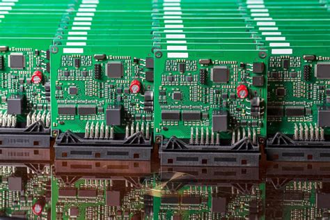
When it comes to pcb manufacturing, implementing cost-effective production techniques can significantly influence your project’s overall success. One of the primary methods to reduce pcb manufacturing cost is to optimize the layout and design of your circuit boards. By minimizing the use of expensive materials and reducing waste, you can achieve substantial savings. Partnering with experienced pcb manufacturing companies can also provide you with valuable insights and access to advanced machinery, ensuring efficient production processes. Additionally, techniques such as panelization, where multiple boards are produced on a single panel, can further reduce costs by streamlining the manufacturing workflow.
Choosing appropriate materials that balance quality and affordability is crucial for any pcb manufacturing business aiming for cost efficiency. High-volume orders often benefit from economies of scale; thus, planning your production cycles carefully can yield financial advantages while maintaining high standards. Adopting automated assembly processes reduces manual labor costs and enhances precision, leading to fewer errors and higher throughput.
Overall, staying informed about industry trends and leveraging innovative technologies will help you maintain a competitive edge while managing costs effectively in pcb manufacturing projects.
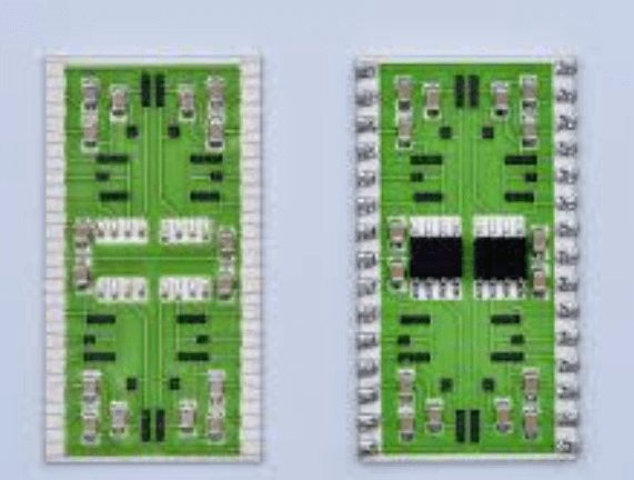
Advanced Materials and Their Applications
In the realm of custom PCB printing, the utilization of advanced materials plays a crucial role in optimizing both functionality and performance. New-age materials such as flexible polymers, ceramic substrates, and advanced composites allow for innovative designs that improve reliability and durability. These materials enable pcb manufacturing companies to push the boundaries of traditional PCB designs, facilitating the development of devices that are thinner, more robust, and capable of withstanding extreme conditions.
Flexible polymers have become particularly popular, offering advantages in terms of bendability and weight reduction. They are ideal for applications requiring dynamic movement or compact assembly. Ceramic substrates excel in high-frequency circuits due to their superior thermal conductivity and stability. Advanced composites blend different materials to achieve improved mechanical strength and electrical performance.
The selection of proper materials directly impacts pcb manufacturing cost as well. While advanced materials may initially seem more expensive, their long-term benefits in terms of durability and performance can lead to cost savings in the entire pcb manufacturing business cycle.
In essence, understanding the properties and applications of advanced materials is pivotal for engineers aiming to enhance their projects’ reliability, efficiency, and overall quality. By leveraging these innovations, you can achieve remarkable results in your custom PCB projects, setting a new standard in the ever-evolving landscape of electronics design and production.
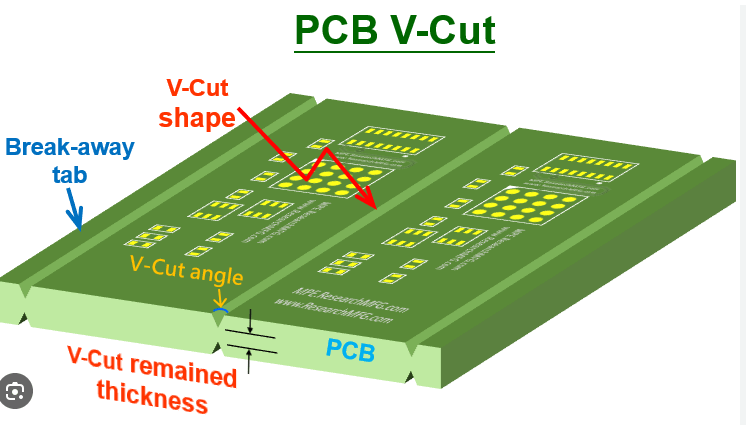
Exploring CNC Milling and Laser Cutting Techniques
When diving into the world of custom PCB printing, understanding CNC milling and laser cutting techniques is crucial for achieving precision and high-quality results. PCB manufacturing has greatly benefited from these advanced methods. CNC milling utilizes computer-controlled machines to create intricate PCB designs, providing unparalleled accuracy by meticulously removing material to form the necessary pathways on the board. On the other hand, laser cutting employs high-powered lasers to cut through PCB materials with exceptional speed and precision, making it ideal for complex and delicate patterns.
One of the primary advantages of utilizing these techniques in pcb manufacturing companies is the ability to produce prototypes rapidly without compromising on quality. This speed ensures that you can test and iterate your designs swiftly, a critical factor in innovative development phases. Furthermore, mastering these techniques can significantly reduce pcb manufacturing cost, as they eliminate many manual errors and material waste associated with traditional methods.
Both CNC milling and laser cutting support a variety of materials used in PCB construction, from standard FR4 to advanced substrates like polyimide or ceramic-based boards. This versatility allows pcb manufacturing business operations to tailor their processes according to specific project requirements, ensuring optimal performance for different electronic applications.
By integrating CNC milling and laser cutting into your custom pcb printing workflow, you’ll enhance your ability to produce superior PCBs that meet stringent quality standards while keeping production costs in check. Adopting these sophisticated techniques not only elevates the capabilities of engineers but also empowers hobbyists keen on advancing their electronic projects.
Innovations in 3D PCB Printing
One of the most groundbreaking developments in PCB manufacturing is the advent of 3D PCB printing. This cutting-edge technique permits the creation of highly complex and three-dimensional circuit boards that were previously impossible to fabricate using traditional methods. PCB manufacturing companies are increasingly adopting 3D printing technology to streamline production processes, reduce errors, and shorten turnaround times. The ability to rapidly prototype with 3D printing significantly lowers pcb manufacturing cost, enabling both large-scale enterprises and small-scale hobbyists to explore innovative designs without breaking the bank. The flexibility offered by 3D printing allows for intricate and compact layouts, which are crucial for modern electronic devices. Whether you’re an established entity in the pcb manufacturing business or an aspiring engineer, integrating 3D PCB printing into your workflow can elevate your project’s capabilities and efficiency.
Optimizing Design for Superior Quality and Performance
In the intricate world of pcb manufacturing, achieving superior quality and performance in your custom PCBs starts with meticulous design optimization. By focusing on critical aspects like trace layout, component placement, and thermal management, you can significantly enhance the functionality and reliability of your boards. Collaborating with pcb manufacturing companies can provide access to advanced design tools and industry insights that streamline this process. It’s also crucial to balance between quality and pcb manufacturing cost: investing in high-quality materials and sophisticated design techniques often translates to improved durability and performance of the final product. Additionally, adopting Design for Manufacturability (DFM) principles allows you to minimize errors during production, ensuring that your PCBs are efficiently manufactured without compromising on quality. For those engaged in the pcb manufacturing business, continually updating design methodologies to incorporate the latest technologies can lead to innovative solutions that push the boundaries of what’s possible in custom PCB projects.
Conclusion
In conclusion, unlocking the vast potential of custom PCB printing requires an understanding of multiple facets from design to production. By embracing rapid prototyping, you can drastically enhance innovation and streamline development cycles. Cost-effective approaches to production ensure that your projects stay within budget while meeting or exceeding quality standards. Leveraging advanced materials broadens the scope of what you can achieve, enhancing both performance and durability.
Techniques such as CNC milling and laser cutting provide precision and flexibility in pcb manufacturing, allowing for intricate designs that standard methods may not support. Likewise, delving into the world of 3D PCB printing opens new avenues for complex and compact designs. To optimize your custom PCB projects for superior quality, engineers and hobbyists alike must adopt a holistic approach that considers both technical intricacies and practical constraints.
PCB manufacturing companies serve as invaluable partners in this journey, offering expertise and resources that can significantly lower the pcb manufacturing cost. Engaging with these entities not only saves time but also equips you with a wealth of knowledge that could propel your pcb manufacturing business to new heights. Therefore, by mastering these elements, you can craft innovative solutions tailored perfectly to your unique needs.
Frequently Asked Questions
Custom PCB printing can often lead to a multitude of questions for both seasoned engineers and hobbyists. Below are some of the most frequently asked questions about this innovative field:
Q: What are the key advantages of custom PCB printing?
A: Custom PCB printing offers tailored solutions that fit specific needs. It grants you the flexibility to design unique electronic devices with precision, ensuring high quality and optimized performance.
Q: How cost-effective is custom PCB printing?
A: The pcb manufacturing cost can be kept low by leveraging advanced techniques such as rapid prototyping and innovative materials. Engaging with leading pcb manufacturing companies ensures economies of scale, reducing overall expenditure.
Q: What is the typical turnaround time for custom PCBs?
A: Turnaround times can vary based on complexity and volume. However, modern technology in pcb manufacturing business often allows for expedited processes, from design to production.
For more detailed information about starting your own projects or modifying existing designs with state-of-the-art techniques, please click here to explore how leading companies optimize their PCB manufacturing processes.