USB high speed pcb design
Optimizing Trace Layout for USB High Speed PCB Design
Optimizing trace layout for USB high-speed PCB design is a critical aspect that demands meticulous attention to detail.
The performance and reliability of USB high-speed circuits are highly dependent on the precision of the trace layout.
To begin with, it is essential to understand that USB high-speed signals operate at frequencies that make them susceptible to signal integrity issues such as crosstalk, reflection, and electromagnetic interference (EMI).
Therefore, the layout must be designed to minimize these potential problems.
One of the primary considerations in optimizing trace layout is maintaining controlled impedance.
Controlled impedance ensures that the signal integrity is preserved as it travels through the PCB traces.
This can be achieved by carefully selecting the trace width, spacing, and the dielectric material of the PCB.
The characteristic impedance of USB high-speed signals is typically 90 ohms differential, and maintaining this impedance is crucial for minimizing signal reflections.
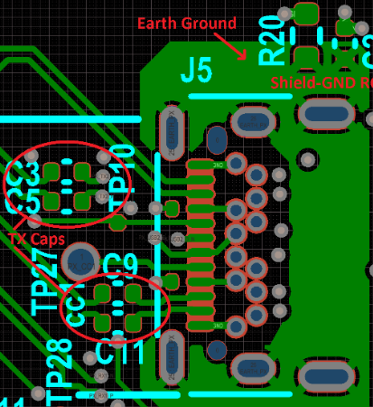
To achieve this, designers often use differential pairs, which consist of two traces that carry the signal and its complement.
These traces should be routed as close together as possible to ensure that they are affected equally by external noise sources, thereby improving noise immunity.
In addition to controlled impedance, trace length matching is another vital factor.
USB high-speed signals require that the lengths of the differential pairs be matched as closely as possible.
Any length mismatch can result in skew, where one signal arrives before the other, leading to data corruption.
To mitigate this, designers should use serpentine routing or meandering techniques to equalize the lengths of the traces.
It is also advisable to keep the traces as short as possible to reduce the potential for signal degradation.
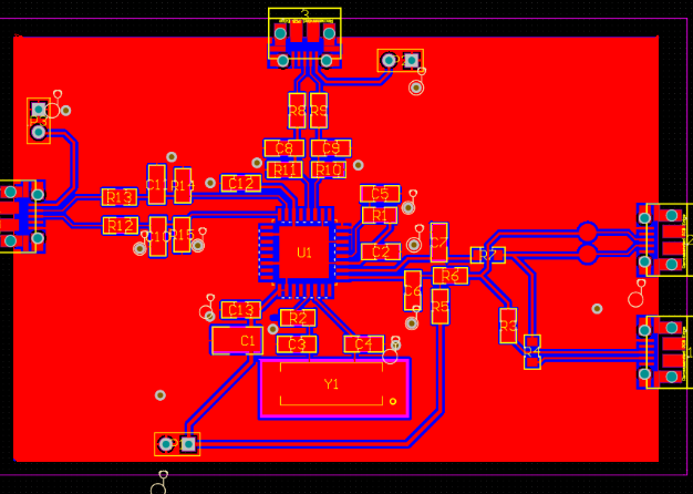
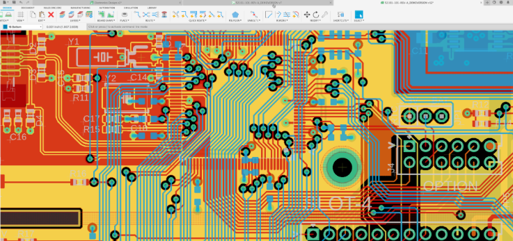
Furthermore, the placement of components plays a significant role in optimizing trace layout.
Critical components such as USB connectors, transceivers, and termination resistors should be placed in close proximity to each other to minimize trace lengths and reduce the potential for signal integrity issues.
Additionally, it is important to avoid placing high-speed traces near noisy components or power supply lines, as this can introduce unwanted interference.
Ground planes are another essential element in high-speed PCB design.
A continuous ground plane provides a low-impedance return path for the high-speed signals, which helps to reduce EMI and improve signal integrity.
It is crucial to ensure that the ground plane is uninterrupted and that there are no splits or gaps beneath the high-speed traces.
This can be achieved by using a multilayer PCB design, where one or more layers are dedicated to the ground plane.
Moreover, proper termination is necessary to prevent signal reflections.
Termination resistors should be placed as close as possible to the receiver end of the differential pairs.
The value of the termination resistors should match the characteristic impedance of the traces to ensure maximum power transfer and minimal reflections.
Lastly, it is important to consider the use of vias in the trace layout.
Vias can introduce impedance discontinuities and signal reflections, so their use should be minimized.
When vias are necessary, they should be placed symmetrically on both traces of the differential pair to maintain balance.
In conclusion, optimizing trace layout for USB high-speed PCB design involves a combination of controlled impedance, trace length matching, strategic component placement, continuous ground planes, proper termination, and careful use of vias.
By adhering to these principles, designers can ensure that their USB high-speed circuits perform reliably and efficiently, thereby meeting the stringent requirements of modern electronic devices.
Importance of Impedance Control in USB High Speed PCB Design
In the realm of USB high-speed PCB design, the importance of impedance control cannot be overstated.
As data transfer rates continue to escalate, the need for precise impedance control becomes increasingly critical to ensure signal integrity and overall system performance. Impedance control refers to the management of the characteristic impedance of the transmission lines on a PCB,
which is essential for minimizing signal reflections and maintaining signal quality.
To begin with, USB high-speed interfaces, such as USB 2.0 and USB 3.0, operate at frequencies where signal integrity issues become prominent.
At these high frequencies, even minor impedance mismatches can lead to significant signal reflections, which in turn cause data corruption and communication errors.
Therefore, maintaining a consistent impedance along the transmission path is crucial for reliable data transfer.
This is achieved by carefully designing the PCB traces to match the characteristic impedance required by the USB standard, typically 90 ohms differential for USB 2.0 and 85 ohms differential for USB 3.0.
Moreover, the PCB material selection plays a pivotal role in impedance control.
The dielectric constant of the PCB substrate affects the impedance of the traces.
High-frequency signals are particularly sensitive to variations in the dielectric constant, which can lead to impedance discontinuities.
Consequently, designers must choose materials with stable dielectric properties and ensure that the manufacturing process maintains these properties consistently across the PCB.
In addition to material selection, the physical dimensions of the PCB traces are critical for impedance control.
The width and spacing of the traces, as well as the thickness of the dielectric layer between the traces and the reference plane, must be precisely controlled.
These parameters are typically determined using impedance calculators or simulation tools, which take into account the specific characteristics of the PCB material and the desired impedance.
By adhering to these calculated dimensions, designers can achieve the target impedance and minimize signal reflections.
Furthermore, the layout of the PCB also influences impedance control.
The routing of high-speed USB signals should be as straight and short as possible to reduce the potential for impedance variations.
Additionally, differential pairs, which are used for high-speed USB signals, must be routed with consistent spacing and length to maintain the differential impedance.
Any deviation in the length or spacing of the differential pairs can result in skew, which degrades signal integrity and can lead to data errors.
Another aspect to consider is the impact of vias on impedance control.
Vias, which are used to connect different layers of a PCB, introduce impedance discontinuities due to their inductive and capacitive properties.
To mitigate this, designers often use techniques such as back-drilling to remove the unused portion of the via, thereby reducing its impact on impedance.
Additionally, careful placement of vias and minimizing their use in high-speed signal paths can help maintain consistent impedance.
In conclusion, impedance control is a fundamental aspect of USB high-speed PCB design that directly affects signal integrity and system performance.
By carefully selecting PCB materials, controlling trace dimensions, optimizing layout, and managing vias, designers can achieve the precise impedance required for reliable high-speed data transfer.
As USB data rates continue to increase, the importance of meticulous impedance control will only grow, underscoring its critical role in the design and manufacturing of high-speed PCBs.
Best Practices for Power and Ground Planes in USB High Speed PCB Design
In the realm of USB high-speed PCB design, the meticulous management of power and ground planes is paramount to ensuring optimal performance and signal integrity.
The design of these planes can significantly influence the overall functionality and reliability of the USB interface, making it essential to adhere to best practices.
To begin with, it is crucial to establish a solid ground plane.
A continuous, unbroken ground plane serves as a reference point for all signals and helps to minimize electromagnetic interference (EMI).
This uninterrupted plane provides a low-impedance path for return currents, which is vital for maintaining signal integrity, especially at high frequencies.
When designing the ground plane, it is advisable to avoid splitting it into multiple sections, as this can create potential differences that lead to noise and signal degradation.
In conjunction with a robust ground plane, the power plane must also be carefully designed.
The power plane should be placed adjacent to the ground plane to form a high-frequency decoupling capacitor.
This proximity helps to reduce the loop inductance and enhances the overall performance of the power distribution network.
Additionally, it is beneficial to use multiple vias to connect the power and ground planes, thereby reducing the impedance and improving the current-carrying capability.
Another critical aspect of power and ground plane design is the placement of decoupling capacitors.
These capacitors should be strategically located close to the power pins of the USB components to filter out high-frequency noise.
The use of a variety of capacitor values can help to cover a broad range of frequencies, ensuring that the power supply remains stable across the entire operating spectrum. Furthermore, the capacitors should be connected with short, wide traces to minimize inductance and resistance.
The layout of the power and ground planes should also consider the return paths of high-speed signals.
Ensuring that these signals have a clear and direct return path on the ground plane is essential to prevent the creation of large current loops, which can act as antennas and radiate EMI.
To achieve this, it is advisable to route high-speed traces over a continuous ground plane and avoid crossing splits or gaps in the plane.
Thermal management is another factor that must be taken into account when designing power and ground planes.
High-speed USB devices can generate significant amounts of heat,
which needs to be dissipated effectively to maintain performance and reliability.
Incorporating thermal vias and copper pours can help to spread the heat more evenly across the PCB, preventing hotspots and ensuring that the components operate within their specified temperature ranges.
In addition to these considerations, it is important to perform thorough simulations and testing during the design process.
Tools such as electromagnetic field solvers and signal integrity simulators can provide valuable insights into the behavior of the power and ground planes,
allowing designers to identify and mitigate potential issues before they become problematic.
Post-fabrication testing, including impedance measurements and EMI testing, can further validate the design and ensure compliance with relevant standards.
In conclusion, the design of power and ground planes in USB high-speed PCB design is a complex but critical task that requires careful attention to detail.
By following best practices such as maintaining continuous planes, strategically placing decoupling capacitors, ensuring clear return paths, managing thermal dissipation, and conducting thorough simulations and testing, designers can achieve a robust and reliable USB interface that meets the demands of high-speed data transmission.
Managing Signal Integrity in USB High Speed PCB Design
Managing signal integrity in USB high-speed PCB design is a critical aspect that demands meticulous attention to detail.
As USB technology continues to evolve, the need for higher data transfer rates has become paramount, necessitating the design of PCBs that can handle these speeds without compromising signal integrity.
Ensuring signal integrity involves a comprehensive understanding of various factors, including impedance control, trace routing, and the minimization of electromagnetic interference (EMI).
To begin with, impedance control is a fundamental aspect of maintaining signal integrity in high-speed USB PCB design.
USB signals are transmitted as differential pairs, and it is crucial to maintain a consistent impedance throughout the signal path.
Any deviation in impedance can result in signal reflections, which can degrade the quality of the signal and lead to data errors.
To achieve this, designers must carefully calculate the trace width and spacing, taking into account the dielectric properties of the PCB material.
Additionally, the use of controlled impedance traces ensures that the signal remains within the desired impedance range, thereby minimizing reflections and maintaining signal integrity.
Moreover, trace routing plays a significant role in managing signal integrity.
High-speed USB signals are susceptible to crosstalk,
which occurs when signals on adjacent traces interfere with each other. To mitigate crosstalk, it is essential to maintain adequate spacing between high-speed traces and to route differential pairs together.
This practice helps to ensure that the signals remain tightly coupled, reducing the likelihood of interference. Furthermore, avoiding sharp bends in the traces and using smooth, gradual curves can help to minimize signal degradation. It is also advisable to keep the trace lengths as short as possible to reduce the potential for signal loss and timing issues.
In addition to impedance control and trace routing, minimizing electromagnetic interference (EMI) is crucial for maintaining signal integrity in high-speed USB PCB design.
EMI can be generated by various sources, including power supplies, clock signals, and other high-speed components.
To reduce EMI, designers should implement proper grounding techniques, such as using a solid ground plane and ensuring that all high-speed signals have a clear return path.
Additionally, the use of decoupling capacitors can help to filter out high-frequency noise and stabilize the power supply, further reducing the potential for EMI.
Another important consideration in managing signal integrity is the selection of appropriate PCB materials.
High-speed USB signals require materials with low dielectric loss and stable dielectric constants to ensure minimal signal attenuation.
Commonly used materials for high-speed designs include FR4, Rogers, and other high-performance laminates.
The choice of material can significantly impact the overall performance of the PCB, and it is essential to select a material that meets the specific requirements of the USB application.
Furthermore, simulation and testing are indispensable tools in the design process.
Signal integrity simulation software can help designers to predict and analyze the behavior of high-speed signals, allowing them to identify potential issues and make necessary adjustments before the PCB is manufactured.
Once the PCB is fabricated, thorough testing using high-speed oscilloscopes and other diagnostic tools is essential to verify that the design meets the required performance standards.
In conclusion, managing signal integrity in USB high-speed PCB design involves a multifaceted approach that encompasses impedance control, trace routing, EMI minimization, material selection, and rigorous testing.
By paying careful attention to these factors, designers can ensure that their PCBs are capable of handling high-speed USB signals with minimal signal degradation, thereby achieving reliable and efficient data transfer.


