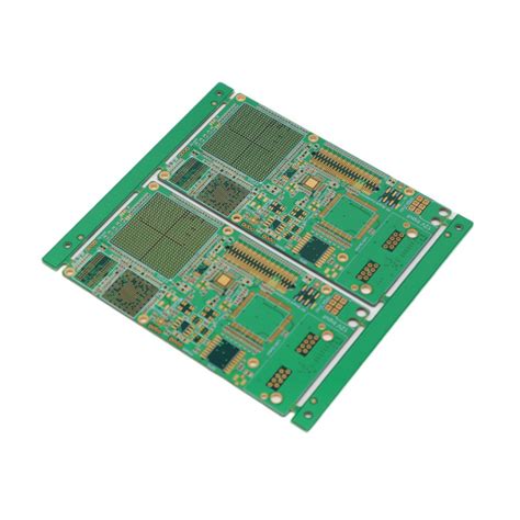
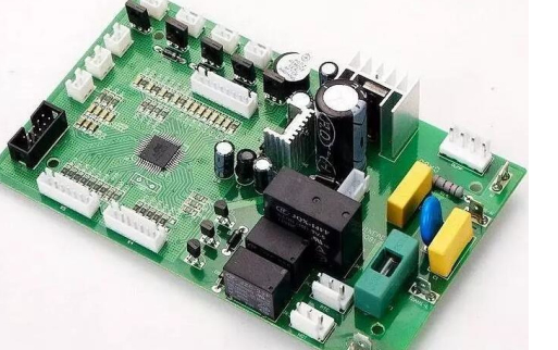
USB PCB Layout Design: Best Practices and Guidelines
Introduction
Universal Serial Bus (USB) has become one of the most widely used interfaces for connecting peripherals to computers and other electronic devices. The USB standard has evolved over the years, from USB 1.0 to the latest USB4, with each iteration bringing higher data transfer rates and improved power delivery capabilities. As the USB standard has advanced, the design of printed circuit boards (PCBs) that incorporate USB interfaces has become increasingly complex. Proper USB PCB layout is critical to ensure reliable data transmission, minimize electromagnetic interference (EMI), and maintain signal integrity.
This article will provide an in-depth look at best practices and guidelines for USB PCB layout design. We will cover topics such as impedance matching, differential pair routing, power delivery, and EMI considerations. By following these guidelines, designers can create robust and reliable USB-enabled PCBs that meet the requirements of modern USB standards.
USB Standards and Their Impact on PCB Layout
Before diving into the specifics of USB PCB layout, it is important to understand the different USB standards and how they impact design considerations. The main USB standards include:
- USB 1.x: Low-speed (1.5 Mbps) and Full-speed (12 Mbps)
- USB 2.0: High-speed (480 Mbps)
- USB 3.x: SuperSpeed (5 Gbps) and SuperSpeed+ (10 Gbps, 20 Gbps)
- USB4: Up to 40 Gbps
As data rates have increased with each new USB standard, the importance of proper PCB layout has grown significantly. Higher data rates require more careful attention to signal integrity, impedance matching, and EMI mitigation.
Impedance Matching
Impedance matching is crucial for maintaining signal integrity in high-speed USB interfaces. The USB specification defines characteristic impedance requirements for differential pairs:
- USB 1.x and USB 2.0: 90 Ω differential impedance
- USB 3.x and USB4: 90 Ω differential impedance with tighter tolerances
To achieve the required impedance, designers must carefully consider:
- Trace width and spacing
- PCB stackup
- Dielectric constant of the PCB material
- Copper thickness
Most PCB design software includes impedance calculation tools that can help determine the appropriate trace dimensions for a given stackup and material.
Differential Pair Routing
USB interfaces use differential signaling to transmit data, which provides better noise immunity and allows for higher data rates compared to single-ended signaling. Proper routing of differential pairs is essential for maintaining signal integrity:
- Keep differential pairs as short as possible
- Maintain consistent spacing between the two traces of a differential pair
- Route differential pairs on the same layer whenever possible
- Avoid vias in differential pairs when possible, as they can introduce impedance discontinuities
- If vias are necessary, use matched pairs and keep stub lengths to a minimum
- Maintain proper spacing between differential pairs and other signals to minimize crosstalk
Power Delivery Considerations
Modern USB standards, particularly USB 3.x and USB4, support higher power delivery capabilities. This requires careful consideration of power distribution in the PCB layout:
- Use appropriate trace widths for power and ground connections
- Implement proper decoupling capacitors near USB connectors and ICs
- Consider using power planes for better current distribution
- Follow USB-IF guidelines for VBUS and GND routing
- Implement proper ESD protection on power lines
EMI Mitigation
High-speed USB interfaces can generate significant electromagnetic interference if not properly designed. To minimize EMI:
- Use ground planes to provide a low-impedance return path
- Implement proper shielding for USB connectors
- Use ferrite beads or common-mode chokes on differential pairs when necessary
- Keep high-speed signals away from board edges
- Use stitching vias to connect ground planes on different layers
- Implement proper filtering on power lines
USB Connector Placement and Routing
The placement of USB connectors on the PCB can significantly impact signal integrity and EMI:
- Place USB connectors near the edge of the board to minimize trace lengths
- Avoid placing connectors near noisy components or switching power supplies
- Provide adequate clearance around connectors for mechanical considerations
- Follow manufacturer recommendations for connector footprint design
- Implement proper grounding for connector shields
Layer Stackup Considerations
The PCB layer stackup plays a crucial role in USB interface performance:
- Use at least a 4-layer board for USB 2.0 and above
- Place high-speed USB signals on inner layers between ground planes when possible
- Use dedicated power and ground planes for better power distribution and EMI control
- Consider using microstrip or stripline configurations for controlled impedance routing
Signal Integrity Analysis
For high-speed USB interfaces, signal integrity analysis is essential:
- Perform pre-layout simulations to determine optimal routing strategies
- Use post-layout simulations to verify signal integrity
- Analyze eye diagrams to ensure compliance with USB specifications
- Consider using time-domain reflectometry (TDR) to verify impedance matching
Testing and Validation
After completing the PCB layout, thorough testing and validation are necessary:
- Perform continuity and isolation tests
- Verify impedance matching using TDR
- Conduct signal integrity tests using high-speed oscilloscopes
- Perform EMI testing to ensure compliance with regulatory requirements
- Validate power delivery capabilities
Common Pitfalls to Avoid
When designing USB PCB layouts, there are several common mistakes to avoid:
- Neglecting impedance matching requirements
- Improper differential pair routing
- Inadequate power distribution and decoupling
- Poor grounding and shielding practices
- Insufficient clearance between high-speed signals and other components
- Overlooking ESD protection requirements
Advanced Considerations for USB4 and Beyond
As USB technology continues to evolve, with USB4 offering speeds up to 40 Gbps, PCB layout considerations become even more critical:
- Implement more stringent impedance control
- Use advanced materials with lower dielectric loss
- Consider using backdrilling to minimize via stubs
- Implement more sophisticated EMI mitigation techniques
- Use advanced simulation tools for signal and power integrity analysis
Conclusion
Designing a robust and reliable USB PCB layout requires careful attention to numerous factors, including impedance matching, differential pair routing, power delivery, and EMI mitigation. As USB standards continue to evolve, with increasing data rates and power delivery capabilities, the importance of proper PCB layout design only grows.
By following the best practices and guidelines outlined in this article, designers can create USB-enabled PCBs that meet the stringent requirements of modern USB standards. Proper design not only ensures reliable operation but also helps to minimize costly redesigns and production delays.
As with any high-speed interface design, thorough testing and validation are essential to ensure that the final product meets all performance and regulatory requirements. By combining careful design practices with comprehensive testing, engineers can create USB interfaces that deliver optimal performance and reliability in a wide range of applications.
Remember that USB PCB layout is both an art and a science, requiring a balance of theoretical knowledge and practical experience. As you gain more experience with USB interface design, you’ll develop a better intuition for identifying and addressing potential issues before they become problems in the final product.


