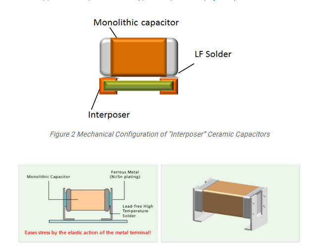
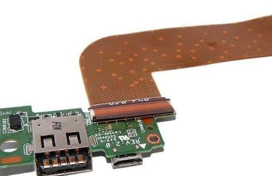
Usb pcb mount
Designing Efficient USB PCB Mounts for Compact Devices
Designing efficient USB PCB mounts for compact devices is a critical aspect of modern electronics engineering. As devices become increasingly smaller and more sophisticated, the need for reliable and space-saving USB connections grows. The process of integrating USB ports into printed circuit boards (PCBs) requires careful consideration of several factors to ensure both functionality and durability.
To begin with, the selection of the appropriate USB connector type is paramount.
USB connectors come in various forms, including Type-A, Type-B, Micro-USB, and USB-C. Each type has its own set of advantages and limitations. For compact devices, USB-C is often the preferred choice due to its small size, reversible design, and high data transfer rates. However, the choice ultimately depends on the specific requirements of the device and its intended use.
Once the connector type is selected, the next step involves the precise placement of the USB port on the PCB.
This placement must account for both mechanical and electrical considerations. Mechanically, the USB port should be positioned to minimize stress on the solder joints and to ensure ease of access for the end user. Electrically, the placement should minimize signal degradation and interference. This often involves placing the USB port as close as possible to the relevant components, such as the microcontroller or power management IC, to reduce trace lengths and potential signal loss.
In addition to placement, the mounting method of the USB connector is crucial.
Surface-mount technology (SMT) and through-hole technology (THT) are the two primary methods used. SMT is favored for its ability to save space and its compatibility with automated assembly processes. However, THT can provide stronger mechanical bonds, which may be necessary for devices subject to frequent physical stress. In some cases, a hybrid approach that combines both SMT and THT can offer the best of both worlds, providing both space efficiency and mechanical robustness.
Thermal management is another important consideration in the design of USB PCB mounts.
USB connectors can generate heat during operation, particularly when transferring large amounts of data or charging devices. Effective thermal management strategies, such as the use of thermal vias and heat sinks, can help dissipate this heat and prevent damage to the PCB and surrounding components. Additionally, careful selection of materials with good thermal conductivity can further enhance heat dissipation.
Signal integrity is also a key factor in designing efficient USB PCB mounts.
High-speed data transfer requires maintaining the integrity of the signal throughout the PCB. This involves careful routing of the differential pairs associated with the USB data lines, ensuring that they are of equal length and avoiding sharp bends that can cause signal reflection. The use of controlled impedance traces and proper grounding techniques can further enhance signal integrity.
Finally, the overall durability and reliability of the USB connection must be considered.
This includes selecting high-quality connectors that can withstand repeated insertions and removals, as well as ensuring that the solder joints are robust and free from defects. Conformal coating or other protective measures can also be employed to protect the USB port and PCB from environmental factors such as moisture and dust.
In conclusion, designing efficient USB PCB mounts for compact devices involves a multifaceted approach that balances mechanical, electrical, and thermal considerations. By carefully selecting the appropriate connector type, optimizing placement and mounting methods, managing thermal and signal integrity, and ensuring overall durability, engineers can create reliable and efficient USB connections that meet the demands of modern compact devices.

Top Challenges in USB PCB Mount Integration and Solutions
Integrating USB connectors into printed circuit boards (PCBs) presents a range of challenges that engineers must navigate to ensure optimal performance and reliability. One of the primary challenges in USB PCB mount integration is maintaining signal integrity. USB signals, particularly those conforming to high-speed standards such as USB 3.0 and USB 3.1, are highly susceptible to noise and interference. To mitigate this, careful attention must be paid to the layout of the PCB. Differential pairs should be routed with consistent spacing and minimal skew to preserve signal quality. Additionally, the use of ground planes and proper shielding can help reduce electromagnetic interference (EMI) and crosstalk between adjacent traces.
Another significant challenge is the mechanical stability of the USB connector.
USB connectors are subject to frequent plugging and unplugging, which can lead to mechanical stress on the solder joints and the PCB itself. To address this, designers often employ through-hole mounting techniques, which provide greater mechanical strength compared to surface-mount technology (SMT). Reinforcing the USB connector with additional solder points or using a combination of through-hole and SMT can further enhance durability. Moreover, selecting connectors with robust housing materials and secure locking mechanisms can help withstand the physical demands of repeated use.
Thermal management is also a critical consideration in USB PCB mount integration.
High-speed USB connectors can generate significant heat, which, if not properly managed, can lead to thermal stress and potential failure of the PCB components. Implementing thermal vias and heat sinks can aid in dissipating heat away from critical areas. Additionally, using materials with high thermal conductivity for the PCB substrate can improve overall thermal performance. Ensuring adequate airflow around the USB connector and the PCB can also help maintain safe operating temperatures.
Power delivery is another area where challenges frequently arise.
USB connectors are not only used for data transfer but also for providing power to connected devices. With the advent of USB Power Delivery (USB PD) standards, which allow for higher power levels, ensuring that the PCB can handle the increased current without overheating or causing voltage drops is essential. This requires careful selection of power traces, connectors, and components that can support the required current levels. Employing thicker copper layers and wider power traces can help manage higher currents more effectively.
Furthermore, compliance with industry standards and regulations is a crucial aspect of USB PCB mount integration.
USB connectors and PCBs must adhere to specific standards to ensure compatibility and interoperability with other devices. This includes meeting electrical, mechanical, and environmental specifications outlined by organizations such as the USB Implementers Forum (USB-IF). Conducting thorough testing and validation during the design and manufacturing process can help identify and address any compliance issues early on.
In conclusion, integrating USB connectors into PCBs involves addressing several key challenges, including maintaining signal integrity, ensuring mechanical stability, managing thermal performance, handling power delivery, and complying with industry standards. By employing strategic design practices, such as careful PCB layout, robust mounting techniques, effective thermal management, and thorough testing, engineers can overcome these challenges and achieve reliable and high-performance USB PCB mount integrations. As technology continues to evolve, staying abreast of the latest advancements and best practices in USB PCB mount integration will be essential for developing cutting-edge electronic devices.
Innovative Materials for Durable USB PCB Mounts
In the realm of modern electronics, the durability and reliability of USB PCB mounts are paramount. As devices become more compact and sophisticated, the materials used in these mounts must evolve to meet the increasing demands for performance and longevity. Innovative materials are at the forefront of this evolution, offering enhanced properties that ensure the stability and functionality of USB connections in a variety of applications.
One of the most significant advancements in this field is the development of high-performance polymers.
These materials, such as polyether ether ketone (PEEK) and liquid crystal polymers (LCP), exhibit exceptional mechanical strength and thermal stability. PEEK, for instance, is renowned for its resistance to wear and chemical degradation, making it an ideal choice for environments where USB PCB mounts are subjected to harsh conditions. Similarly, LCPs offer excellent dimensional stability and low moisture absorption, which are critical for maintaining the integrity of the mount over time.
Transitioning from traditional materials like standard plastics to these advanced polymers not only enhances the durability of USB PCB mounts but also improves their performance.
High-performance polymers can withstand higher temperatures, which is particularly beneficial in applications where heat dissipation is a concern. This thermal resilience ensures that the mounts do not deform or lose their structural integrity, thereby maintaining a secure connection between the USB port and the PCB.
In addition to polymers, metal alloys are also being explored for their potential in creating robust USB PCB mounts.
Alloys such as stainless steel and aluminum offer superior strength and rigidity compared to plastic counterparts. Stainless steel, with its excellent corrosion resistance, is particularly suitable for applications in industrial and outdoor environments. Aluminum, on the other hand, provides a lightweight yet sturdy option, which is advantageous in portable electronic devices where weight is a critical factor.
Moreover, the integration of composite materials is another innovative approach gaining traction.
Composites combine the best properties of different materials to create mounts that are both strong and lightweight. For example, carbon fiber-reinforced polymers (CFRPs) are being utilized to produce USB PCB mounts that offer high tensile strength and low weight. This combination is particularly beneficial in aerospace and automotive industries, where reducing weight without compromising strength is essential.
Furthermore, advancements in additive manufacturing, commonly known as 3D printing, are revolutionizing the production of USB PCB mounts.
This technology allows for the creation of complex geometries that are not feasible with traditional manufacturing methods. By using materials such as high-performance thermoplastics and metal powders, 3D printing enables the production of custom mounts that meet specific design requirements and performance criteria. This flexibility in design and material selection opens up new possibilities for optimizing the functionality and durability of USB PCB mounts.
In conclusion, the ongoing development of innovative materials is significantly enhancing the durability and performance of USB PCB mounts. High-performance polymers, metal alloys, composite materials, and advanced manufacturing techniques are all contributing to the creation of more reliable and robust mounts. As technology continues to advance, the materials used in these critical components will undoubtedly evolve further, ensuring that USB connections remain stable and efficient in an ever-expanding range of applications.
Step-by-Step Guide to Soldering USB Connectors on PCBs
Soldering USB connectors onto printed circuit boards (PCBs) is a critical skill for electronics enthusiasts and professionals alike. This process, while seemingly straightforward, requires precision and attention to detail to ensure a reliable and durable connection. To begin with, it is essential to gather all necessary tools and materials. These include a soldering iron, solder wire, flux, a pair of tweezers, a desoldering pump or braid, and, of course, the USB connectors and PCBs.
First and foremost, it is crucial to prepare the workspace.
A clean, well-lit area free from clutter will facilitate a smoother soldering process. Additionally, ensuring proper ventilation is important to avoid inhaling any fumes generated during soldering. Once the workspace is set up, the next step involves preparing the PCB. This entails cleaning the board to remove any dust or contaminants that could interfere with the soldering process. A simple wipe with isopropyl alcohol and a lint-free cloth will suffice.
Following the preparation of the PCB, attention must be turned to the USB connectors.
Inspect the connectors for any visible defects or damage. It is also advisable to pre-tin the connector pins. Pre-tinning involves applying a small amount of solder to the pins before they are placed on the PCB. This step ensures a better bond between the pins and the PCB pads, making the soldering process more efficient.
With the PCB and USB connectors ready, the next step is to align the connector with the designated pads on the PCB.
This alignment is critical, as any misalignment can lead to poor connections or even damage to the PCB. Using tweezers can help in precisely positioning the connector. Once aligned, it is beneficial to secure the connector temporarily with a small amount of solder on one or two pins. This will hold the connector in place while the remaining pins are soldered.
The actual soldering process begins by heating the soldering iron to the appropriate temperature, typically around 350°C (662°F).
Applying a small amount of flux to the pads and pins will help the solder flow more smoothly and create a stronger bond. With the soldering iron heated, touch the tip to both the pad and the pin simultaneously, then introduce the solder wire. The solder should flow and cover the joint, creating a shiny, concave fillet. It is important to avoid using too much solder, as this can create bridges between pins and cause short circuits.
After soldering all the pins, it is prudent to inspect the joints for any cold solder joints or bridges.
Cold solder joints appear dull and may not provide a reliable connection. If any issues are found, they can be corrected by reheating the joint and adding a small amount of solder. In the case of solder bridges, a desoldering pump or braid can be used to remove the excess solder.
Once satisfied with the solder joints, the final step is to clean the PCB again to remove any residual flux. This can be done using isopropyl alcohol and a brush. Cleaning ensures that no corrosive flux remains on the board, which could potentially damage the PCB over time.
In conclusion, soldering USB connectors onto PCBs is a meticulous process that requires careful preparation, precise alignment, and thorough inspection. By following these steps diligently, one can achieve reliable and durable connections, ensuring the proper functioning of the electronic device.